• Please review our updated Terms and Rules here

PDP8/M M8310 problems

MauriceH

Experienced Member
Joined
Apr 2, 2014
Messages
399
Location
Dordrecht , Netherlands
Have the PDP8/M and after some debugging and finally changing out The M8310 board I definitively know this board has a defect.
Even the simple check will fail with this board.
AC Increment
200 7001 increment Ac
201 2300 increment & skip if zero (ISZ)
202 5201 Jump 201
203 5200 Jump 200

At run the machine halt at address 0002 with AC 0000, MD 7402
Status, Link=1
State: F D E IR0 IR1 IR2 MD..
0 1 0 0 1 1 1 0 0 0 0 0

Starting at Single Step adres 200
Memory adr -- AC --- MD
0001 ...........0000...7001
0201............0000...0000
300..............0000...2300
202.............0000....0612
201............0000....5201
203..........2300....2300
200.........2300....5200

So think the problem is with AC increment,AC should become 0001 instead of zero.
Jump instruction seems to work.As in single step the jump is made to 300, So think the instruction 7001 is false.
Checked several IC's like 7474's,E40,E45,E50 and some logic's like E18.E19, E38 concerning AC lines.
Debugged lot of other logic so far no luck to find a defective one (Think it will be the last I ever will check :grin:)

Any Idea's would help.

Maurice
 
From your single step it looks like the ISZ's aren't working right either.
 
Looks like you are not single stepping instructions, but cycles to me.
That's why you see address 300. The ISZ is referring to that address, so you'll have a cycle where you are hitting that address. But there are several strange things, it seems.
The IAC certainly don't look like it works, and neither the ISZ.
 
0200 7001
0201 5200
Single stepping:

0200-start
M Adres.. AC.....MD
001........0000...7001
201........0000...0000
200........0000...5200
202........7001...7001
201........7001...5201
203........4201...5200
200........4201...5200
204........3202...7001
202.......3202...5201
205......0403...5201
040......0403...7440
7402...0403...7402
 
What a job it is! De-soldered several ICs to check on breadboard, Also checking in circuit several main logic paths,Damm that's hard work. All common suspicious FF 7474 taken out,
Took E46 8251 out and tested separately. But I Will Find that Defective IC, So far only find working blocks, haha. I'l keep digging till the last one.
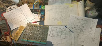
IMG202108252300-M8310-Rep.jpg - Click image for larger version  Name:	IMG202108252300-M8310-Rep.jpg Views:	0 Size:	173.7 KB ID:	1222382
 
So Inspected ALL logical devices, No Luck. Did app. half by tracing on board logic or about a 20 soldered out and checked on breadboard by inputs pulling High by resistors and drawing outputs current with LEDs.SO trying to eliminate static "fake"High and Low. But checked every logic component!!

As the last one checked and finding no defective logic I started the easiest component to check, The TRANSISTOR! LOL Defect! Haha.
Ok than I had a RUNing light again But!! Still No AC-counting.

So Start to check again Those FF 7474's E40,E45,E50.
E40 had a very tricky failure at 2nd FF !! SET, Reset OK, At D is High and Clock Yeb changed the outputs, BUT when I made D LOW, the output Did Not change, With set reset it changes, But NOT when D-is LOW. What a bogger that E40!
Ok changed out E40
Still No AC-count

At start AC becomes 0001 now, RUN light is ON, But it hangs.
Mem Address about 0303 AC=0001 MD=1111 (At M Add I see some LEDs bit dimm also MD so some fast random )
With HALT at that moment M Addres 0201 AC-=0001 MD=5200
Status = 0000
State = 4540

Then Single STEP:AC increase program
0200 start
0201 AC=0001 MD=7001
0202 AC=0001 MD=5201
Status=0000
State= 100 101 100 000

Then made the sugested
200 7001
201 5200
(also zero's MEM locations 0000 till something like adress 0100 and zero's first 200-310,so no false old mem contents)

200 with single step
201 AC=0001 MD= 7001
000 AC=0001 MD=0000
204 AC=0001 MD=0000
000 AC=0001 MD=0000
206 AC=0001 MD=0000
000 AC=0001 MD=0000
210 AC=0001 MD=0000
etc.

Then made the JMP test Program.
That Runs and stop at address 213 MD=7402
instead of 215.

So there is progress. JMP failure I think.
Now I think there still is something perhaps an other tricky Logic that I did not tested thorough enough see the E40 tricky thing.
Damm this M8310 board has got me quite, never had suge a struggle.
 
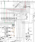
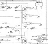
Schematic States E40,E45,E50 an 74H74, I placed a 7474N(E40), The E40,45 is an DEC74H74.E50 an N7474A
Or can I just put in a 74LS74.
Alway's bit confuse about when they can be changed out or not, while has to do with follow up logic.

E404550-M8310.jpg
 

Attachments

  • E404550-M8310.jpg
    E404550-M8310.jpg
    204.2 KB · Views: 1
So Inspected ALL logical devices, No Luck. Did app. half by tracing on board logic or about a 20 soldered out and checked on breadboard by inputs pulling High by resistors and drawing outputs current with LEDs.SO trying to eliminate static "fake"High and Low. But checked every logic component!!

Hi Maurice,

I am very curious about your technique for desoldering 20 ICs. Could you please explain how exactly you do it?

I have been desoldering a few ICs in my Lab-8/e but because all the leads are bent to hold the IC in place during the wave soldering process it is next to impossible using both of my desoldering tools. One of the tools is a soldering station with a hollow tip and a vacuum pump but it is not working with the bent pins. The other is a nice temperature controlled hot air type desolder tool. It melts the solder for all the pins nicely, but then you struggle badly to pull out the IC because you pull against 14 or 16 bent pins while trying to maintain the temperature on the solder side.

I ended up cutting all pins on ICs I wanted to replace and then unsolder one pin at a time with an ordinary soldering station and tweezers. This of course gives you no opportunity to test the ICs on a breadboard like you did - you have to use a new replacement IC (which can be tricky for some of them).

It may be that by the time the PDP-8/m arrived DEC manufacturing no longer bent all IC pins to keep them in place during soldering.

So I would be really grateful to learn about your method.

Thanks and best regards
Tom Hunter
 
Tom cutting is a good option if you know its a defective one.
I use a desolding Iron with vacuum pomp. Then I also use Solder-Wick Desolder Braid from Chemtronics. (Don's buy that crapp from Ali that does not work propper)
That will take the last bit of Tin Out.

For example look for a WELLER WDD 81V. I have a very old type of this kind.
I vacuum from the solder side and at the same time with that vaccuum iron I use it to strait bent those legs.
Then with Solder-Wick at the component side and also pushing the legs a bit back to the IC-Housing I loosen the legs one by one.
Then use a small screwdriver under the IC housing, Wikkel a bit to see if indeed all legs are lose, If not use the normal solder iron to heat up
leg by leg.
Be careful at those PCB though holes that is.

If you get the hand out of it, those IC's are out in a few minutes.
And Clean enough to put them into a Braid board for testing.
Therefore I also use a an IC socket for ease at that braidboard.

That is in this search you want to know if you indeed found a defective one already.

I did not all incicuit test logic due to the fact its a big job tracing all components to get 1 port f.i.LOW to test a Triple-NAND.
Some times you have to probe several lines and lot of logic.

But I did it quite a lot just to be sure great deal of logic is indeed working ON the board it self.
Just finished testing complete JMP path.
That's OK including the FF-s.

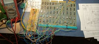
M8310-test setup.jpg - Click image for larger version  Name:	M8310-test setup.jpg Views:	0 Size:	187.4 KB ID:	1223024
 
Schematic States E40,E45,E50 an 74H74, I placed a 7474N(E40), The E40,45 is an DEC74H74.E50 an N7474A
Or can I just put in a 74LS74.
Alway's bit confuse about when they can be changed out or not, while has to do with follow up logic.

They would not have used an H unless it was necessary. Higher cost and more power/heat. The drive in this case is probably not the important thing. It is the speed. The LS parts are quite a lot slower than the H. The S parts should work at an additional cost in power and heat. Surprisingly the input load is similar for the H and S parts so I expect that would not be an issue. Also the average supply current is 15ma on both parts. The S part is about twice as fast as the H. The LS part is about 2/3 the speed of the H. The 7474 is about half the speed of the 74H74. The outputs are all driving just one input so I don't think the output drive matters. Even an L part can drive a single input adequately.

In Summary:

It is possible an LS would work. I can't guarantee it and I would not suggest it. For the gates I can see in the schematic you provided it looks like there should be no problem using a 74S74. DEC would not have used them because they cost more. I really doubt that a 7474 would work. It is half the speed of the 74H74 and if it would work DEC would have used it for the cost savings.

Hope that helps!
 
The 74F series might be reasonable candidates to replace 74H & S if you could not find H and S types, which seem to be getting rarer these days.

Over the years working on vintage pcb's of all kinds, mostly I try to assess the ICs function (of non socketed IC's) in circuit on the pcb they are in, as a way of avoiding a combination of unnecessary removal of a good IC and possible thermal and track damage to the vintage pcb itself.

Making sure as much as possible, with the scope, that the IC is obeying its logic table. Mostly, when an anomalous logic level is found, it almost always turns out that it is the fault of the output stage in the chip driving the line that is defective, rather than the inputs it is connected to loading it down.

The method of "in circuit testing" though is always more difficult when IC lines share a common bus, and one is defective, say holding a line low.

Usually I only remove the IC from a pcb when I have fairly solid evidence it is faulty, then it is not as much of a risk, or a loss of an original vintage part, cutting off its pins prior to removing them as a method to put the pcb's welfare in front of the IC. Most of the time I can remove IC's with the solder sucker and save the IC, but my theory is I shouldn't be removing the non socketed IC at all, if there is any reasonable chance it is still ok and certainly not just for testing. There has to be good test evidence to justify it.

I have always thought that global shotgun removal of IC's for testing was a very bad idea when they are not socketed. Not a bad idea at all to test socketed RAM IC's and socketed IC's that share a common bus. The "the rules" are different depending on the circumstances.

I like to have my vintage pcb's look period correct, so when I replace a failed part, I hunt for a replacement with similar date codes, but I might be an eccentric lunatic in this respect.

One IC failure mode I have come across more recently than I have ever seen in the distant past for 74 TTL's, is an input inside the IC going open circuit and the IC behaving as though that pin is logic high. I have seen this now in both hex inverter gates and Nand gates and in the case of Nand gates, or other logic gates, it can cause chaos because the output of the gate becomes active at times when it shouldn't. There is some sort of aging and destructive process inside 74TTL's that causes this damage and breaking the internal connections from the package pin to the die.
 
I'm impressed with your module debug/test setup. I presume it's because you don't have a W987A quad extender and 3 of those white, flat, flex-cables (where the H851's would go)? Various DEC compatible extenders are available from Todd Goodman, but those white, flat, flex-cables (for the top connectors) seem to be quite rare. Maybe someone will design a replacement using ECS 2418 connectors and 80-conductor Ultra DMA flat ribbon cable?
 
GOT IT WORKING:p:p:p:p:p:p:p:p:p:p:p:p:p!!!!

Pfff what a struggle it was, BUT great succes.
Did swap The DEC74H74 E45 Back , It was OK.But due to suspicious I changed it to 7474N
E50 Back Also to the original 74H74
The Defective E40 74H74 now changed to an 74F74,
Still no result.

Checking again and thinking must be something with that SKIP line.
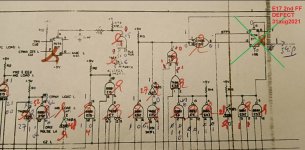
THAN I took out E17 a 7474N, THAT one had a Defective 2nd FF !! I for sure tested that in circuit.
Problem was testing now on braid-board that it though did NOT switched proper.
So changed that to be sure for a 74F74 (Fast logic) .
And finely the PDP8M went on line,

So Defects were Transistor Q1 , E40 and E17. Both FFs.

Next the M6850 Async Comm, that card will not receive, sending it does but corrupt.
Did already some debug, but no luck so far.
Luckily sofar the M6855 is working so could attach VT220, Teletype ASR33 or the Facit 4030 fast tape reader (1200Bd)

Now hoping the RX01 card M8357 will work immediately, and the M847 with already bootstrapped to RX01.
First have to "steal"' the RX02 drive from the PDP1123 at my brothers house and strap it to RX01.
If any body located in EU and has a spare RX01? Would be great.
Or know a conversion from f.i. a physic Shurgard FF 8" drive SA801.
M8310-E17 2eFF-Defect_31aug2021.jpg
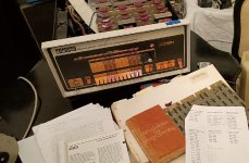
M8310-Werkt3-AC-Increment_31aug2021.jpg
 
Thanks for the Tips about those Top header extentions.
Have the 2x raser cards
Those top headers I have Incomplete set I got from Roland(NL) a couple to start with, many thanks but he run out and I have indeed to complete the set for more convenient testing.
Also have to solder the headers and make flatcables, no problem, but a job on the to do list.
Have some H connection headers I could use for that purpose to complete but I thought I do it the hard way,
And Yes I will order extra to complete the Top header extention set.

Before I dismantled couple of times the PDP8M front panel to test the M8310 with the Bus Load card, But As I got a
working M8310 card temporary from Roland and pdp8M was for now working I'd liked to play with it finely.
But off course as I now for sure knew that the problem was in this M8310 card I started to deep debug that card by "hand".

Former I had already to repair the Front panel and the timing M8330 card. That went all fine but not quit sure
I got all trouble out of it.
Now with a lent out test card M8310 it was much easier to point out the problems.

As I got this PDP8M as an old scrappy machine from an attic or basement app. 10yr ago.
Completely dead on arrival.
Power supply defect, Frontpanel, Timing and so this M8310.
 
Hi Maurice, well done! Always pay good attention to the 74H chips... High speed and high output current. A standard 74xx is often not the right replacement here and might even be not pin compatible...

You can also use a RX01/RX02 floppy emulator to run the machine. And you can add a second floppy drive+controller to the machine. Then you do not have to stress the original drive. And an emulator is blazing fast for booting the machine.

Oh and you have the bare controller board for your TU60 drive. With that you can run CAPS8 from cassette. CAPS8 needs very little memory. Jos Dreesen printed the new rubbers for the capstan for me. This is still working great in my drive!

Regards, Roland
 
Back
Top