• Please review our updated Terms and Rules here

New Tektronix 4051 owner - needs help repairing his 4051

nikola-wan

Veteran Member
Joined
Mar 7, 2018
Messages
1,298
Location
Texas, USA
My collaborator on the Tektronix 4924 GPIB Tape Emulator just acquired a Tektronix 4051 that needs repair.

Here is a set of photos of his new computer:

Front.jpg Rear.jpg

It is in great mechanical shape, and after checking and adjusting the power supplies per the service manuals it has high voltage working but all the status lights on the right of the screen are on - indicating the BASIC ROM did not power up completely.

power up screen won't clear.jpg

Since his 4051 has the extended memory option board to add 24KB of DRAM to the main board 8KB of DRAM, I suggested he unplug the extended memory board and exchange DRAMs with the main memory to see if he had a DRAM problem.

He did that and had no change.

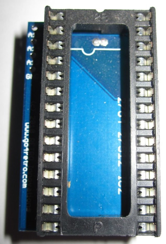
I then have suggested he dump each of the Motorola MCM6832 2Kx8 BASIC ROMs and compare them to the uploaded 4051 BASIC ROM files on bitsavers.org. I pointed him to my Arduino program that I used to dump the MCM6832 ROMs in my Tektronix 4907 GPIB Floppy Drive system:

https://github.com/mmcgraw74/Tektro...ster/4907-Floppy-Drive/ROMs/4907RomReader.ino

Of course my program needs to be modified slightly to change the start address to 0.

My Arduino program was designed to dump all the ROMs while plugged into the 4907 ROM board - since the 4907 ROM board contains an FPLA that patched some of the ROM addresses.
 

Attachments

  • Front.jpg
    Front.jpg
    149.6 KB · Views: 6
If it is a BAD ROM, it looks like a socket adapter to a more available EPROM may be possible.

oldcomputerexpert indicated he had made such an adapter for his 4051:
https://www.vcfed.org/forum/forum/genres/other/65705-tektronix-4051-4052-4052a-4054-4054a-program-archives?p=887036#post887036

Here is an example adapter for a 2364 that would have to be extensively rewired to work:
IMG_2088__75363.1291790006.1280.1280.JPG


from this site: http://store.go4retro.com/2364-adapter/
 
Ahh. That’s the one that sold in UK a few days ago, right?

Now my 4051 had a working main board so I never spent much time on the that one.

Generally speaking I always check the clock signal to the CPU as #1. Then I check the reset circuitry as #2. #3: Is there any chip that gets unusually hot? Perhaps due to bus-contention #4: Does the databus look right? VMA and R/W? Toggling? Seemlingy correct levels? Similar check on address bus. If this looks about right I usually attach a logic analyzer on address- and databus trying to figure out if it execute the correct instructions from reset.
 
I'll check the schematics later - but Mattis is stating exactly how I would attack this.

Just wondering whether building a 6800 NOP generator would be the next step (in the same way that we would with a 6502 PET)? This would be either a 'socket-sandwich' with the 6800 CPU databus being 'jammed' with $01 or a sacrificial 6800 CPU with the databus pins bent out of the socket and pulled up or down to make the value $01. The hope is that the CPU will read a start vector of $0101 and will then continue to execute NOP instructions throughout the 64K address space. However, this is dependent upon the specifics of the I/O sub-system. I will have a look.

The NOP generator would permit assessment of the address decoding logic and would also permit assessment of databus contention.

I would also check the state of the CPU pins /NMI (pin 6) and /IRQ (pin 4) in addition to the clock(s) (pins 3 and 37) and /RESET (pin 40). There should be no permanent /IRQ or /NMI (not permanently LOW); there should be a healthy clock signal and the /RESET should be normally high (but a pulse LOW should be observed on power-up).

Dave
 
I'll check the schematics later - but Mattis is stating exactly how I would attack this.

I would also check the state of the CPU pins /NMI (pin 6) and /IRQ (pin 4) in addition to the clock(s) (pins 3 and 37) and /RESET (pin 40). There should be no permanent /IRQ or /NMI (not permanently LOW); there should be a healthy clock signal and the /RESET should be normally high (but a pulse LOW should be observed on power-up).

Dave

I'm posting this for him as he doesn't have posting privileges yet:

"I found that both IRQ and NMI were LOW. RESET is HIGH. I am uncertain as to what the status should be of some of the other pins mentioned (e.g. VMA and R/W) or how to go about some of the diagnostic steps mentioned by MattisLind but I will post some information on vcfed as soon as I am able to do so."
 
No problem.

I'll check my schematics tonight and post some simple steps for you. We'll go slowly...

However, /NMI and /IRQ being LOW is a problem to start with. We will start here!

VMA and R/W should be oscillating up and down - and not be static. Do you see a clock on pins 3 and 37 of the 6800 CPU? If so, what frequency is it? I suppose I should ask what test equipment you have access to...

Are you in the UK - or did it make a trip overseas?

Monty's a good postman! Hi Monty :)!

I am still snowed under with work - I am just writing this to save myself from going mad. I really want to retire so I can concentrate a bit more on my own projects. Although, from what other people have been saying to me, when you retire you end up with less time for private projects rather than more?!

Dave
 
Hi Dave!! I think the old saying is true - I haven't retired yet either. But I make time for my private projects.

Here are his answers to your questions:

"
Q. VMA and R/W should be oscillating up and down - and not be static.
A. Both VMA and R/W have fluctuating square wave pulses, i.e NOT a static clean square wave but fluctuating pulses. They are at the correct logic level, just a little lower than 5V.

Q. Do you see a clock on pins 3 and 37 of the 6800 CPU? If so, what frequency is it?
A. Yes, on both at 1.205μS (as measured on the 468, translates to approximately 0.833MHz). Again, the waveform is at the correct amplitude.

Q. I suppose I should ask what test equipment you have access to...
For the above I was using the Tek 486 oscilloscope I repaired some time ago. Seemed kind of appropriate but I do also have access to a Rigol 1054Z. In addition I have a DMM and one of those cheap USB LA's off eBay. I am considering the purchase of an EEPROM burner, e.g. TL866II but haven't decided yet.

Q. Are you in the UK - or did it make a trip overseas?
I am in the UK and I drove to London to collect the 4051, so not couriers involved, at least for this purchase.
"
 
I work with 60's to 80's computers with my day job - so (unfortunately) the last thing I want to do is to work with them also when I get home! Hence (alas) the slowness of some of my projects... I aim occasionally 'forced' to take some leave - that's when my own stuff gets done!

I am in sunny Worcester...

It seems as though you know what you are doing - and have the requisite test equipment (better than mine)...

VMA and R/W seem good. A clock of 0.8333 MHz is also good (very good in fact). So with a clock and VMA/R/W toggling we know the CPU is doing something.

Let's find out if it really does reset...

With your test equipment connected to the /RESET pin of the CPU (pin 40); power OFF the machine and let it sit for a while. When you turn it ON, you should notice the /RESET line being held LOW for a while and then going HIGH. This would indicate that the power-on-reset is really working and the CPU should be starting up correctly.

The /NMI line is sourced from two places - U361B (MC6820) and U561B (MC6820). One (or both) of these are driving the /NMI signal LOW. We can't find out (easily) which one - as they are wire-OR'd together. It could be because one (or both) of these devices are faulty, the CPU is not programming them correctly, or because they are being driven incorrectly by the tape interface circuitry (this is what these two devices interface with). Let me think about this one for a while...

EDIT: Are these devices in sockets or not? If they are, you could remove both of them and make sure /NMI goes HIGH and then install them one at a time until you see the /NMI signal on the CPU go permanently LOW. At least it will identify one or the other device... You could always purchase some replacements just in case it is one of the devices?

There are a couple of other things we can do in the meantime. By the way (before I start rambling on further about chip numbers) do you have the schematics for the 4051?

The ROMs are decode by a 74154 4-to-16 decoder (U291). I would probe around the outputs to see which pins (if any) are pulsing LOW. This would indicate which ROM devices code is being executed from (or read out of).

The other simple thing to look at would be the address buffers (U231, U251 and U261). In these cases the signals going into the buffer/drivers should be the same as what is coming out (but only when the two enable inputs - pins 1 and 15 - are LOW). These are driven from pin 7 (BA) of the 6800 CPU. This CPU pin should be LOW.

There are also the data bus buffers (U153 and U163) but these are bidirectional and I will need to think about this a bit more.

Is what I am writing making sense to you or not? I am just trying to gauge how high/low level to pitch my posts at.

EDIT: I notice from the photograph you may have an expansion pack plugged in. Can you remove it please (just in case that is faulty).

Dave
 
Last edited:
Another simple thing, the -5V supply.

This is derived on the CPU board for both the ROMs and RAMs separately (from the -12V). So the PSU low voltage DC supplies may be good - but the ROM and/or RAM supplies not. Can I suggest that you pick a single ROM and RAM and check the DC power supplies on the pins of each chosen device.
 
I think it does. I seemed to remember I had to include for this in my 4051 emulator...

LOADED-1 on J2-19 and TAPE_DATA_1 have both been 'bodged' within my emulator.

Dave
 
Last edited:
Here are the latest responses, hopefully he will be granted access to post soon:

" I am following the discussion and do have volume 2 of the service manual which contains layout and circuit diagrams. I have just dug out the layout diagram to locate the chips being referred to. I can also confirm that I noted BA as being LOW as indicated. I will perform the suggested RESET and other tests tomorrow. I should also add that the memory expansion board and the ROM expansion pack have been removed and have not been plugged in for any of the tests up to this point. Only the display, keyboard and tape drive are connected. I kept the tape drive attached for exactly the reason stated - in case its absence prevented boot-up.

In the meantime, I am also setting up to read the EEPROMs using Monty's sketch for the Arduino Mega. I think it a good idea to check them and capture their content in any case."
 
Well, we seem to have most of the individual ‘bits’ of the equation to get the machine running...

Dave
 
More 4051 troubleshooting update information from John - he is still unable to post directly to vcfed.org.

Done a lot of work this morning. Too much information to post here, however, here is a summary some of the interesting findings.

I have found that RESET is permanently HIGH from switch on. Unless its a short transient, there is no obvious initial LOW period. Not quite sure what "RESTART-O (-15)" refers to on the circuit diagram (page 04_02-03) or what the dotted logic gate is yet. The signal at P14+P15 is a random (in amplitude and duty cycle) square wave pattern. I expecting to find a logic state (HIGH or LOW). The pattern is identical on both pins. Pin 15 is shown as connecting to GND. It does not. Pin 16 is GND.
Scope photo1.jpg

NMI is randomly high and then a slight click can be heard and it goes low. Not sure where the click is coming from. I haven't tried extracting U361B or U561B yet, but yes, they are socketed.

There are other results to report but I really need access to the thread on VCFED. Unfortunately I am still unable to post! Is this meant to encourage members to join?


And then an hour later he reported this:

Something just let go in the power supply letting out the magic smoke so I am stuffed for now. Will need to investigate.
 

Attachments

  • Scope photo1.jpg
    Scope photo1.jpg
    174.8 KB · Views: 1
My 4052 display board tantalum capacitors were one of my issues with blowing the power supply fuses.

Check out the display board where the power comes in - the 4052 Display Board is identical to the 4051 display board and has small tantalum capacitors near where the power enters the display board. I replaced all of those capacitors.

Here is a link to my 4052 troubleshooting post: https://www.vcfed.org/forum/forum/genres/other/64617-tektronix-4052-troubleshooting#post64617
 
Update on his power supply troubleshooting:

Have investigated the power supply. Looks like a diode on the 20V rail (CR331) has failed. This appears to have led to the failure of the bridge rectifier CR32 which has a crack along its top. My slip with the probe when measuring voltages on the fuses might have precipitated this. I have replaced the diode, but will have to order a suitable rectifier or else fudge it with 1N5404's I have to hand.

The Tektronix 4051 service manual only lists a Tektronix part number for the C32 bridge rectifier and 200V 3A spec.
The Tektronix Semiconductor Design Catalog is available on https://w140.com/Tektronix_Xref_sm.pdf but does not list any cross reference parts, just has a diagram of the component size and W675 family (?).

I happen to have a spare 4051 power supply that came with some 4052 parts. The CR32 rectifier is labeled as a Varo VH247.
Here is a link to a surplus site page for the Varo VH247 but they have no stock: https://www.electronicsurplus.com/varo-vh247-diode-fwb-200v-6amp Their webpage indicates this is a 6A part.

I found a Varo 1982 Bridge Rectifier catalog: here is the VH247 page:

Varo VH247 datasheet.jpg
 
Tantalum bead capacitor == Smurf Grenade (as Brad calls them). LOL...

RESTART-0 (-15) means it is a signal called RESTART (he says, stating the obvious). The -0 means it is active low. A -1 would mean active high. The -15 means drawing sheet number 15 on the same board.

If you look in the maintenance manual you will find a complete cross-reference for all of the signal names. The Tektronix maintenance manuals are very comprehensive...

New people are moderated for their first 10 (or so) posts. We have just had a software ‘upgrade’ to the forum and everyone (moderators included) are feeling the pain at the moment. Please stick with the posting and one of the moderators will get you sorted out when they have some time. Everyone is a volunteer, and they have real lives as well as us! The advantage of this is very real for us users, as it keeps the forum pretty clear of spam. So, I think, the benefits outweigh the disbenefits - unless you are the one being moderated of course!

Monty’s the Tek power supply guru.

Right, I have done the gardening I was planning to do today, so back to my 4052 emulator keyboard problem...

Dave
 
Thanks to some assistance I now have the ability to write something. Yey! Apparently I should have received a verification e-mail that never materialised so my account was never verified, hence no privileges. Now that I can respond (moderation notwithstanding), firstly, let me say thank you to everyone who responded to the request started by Monty for help with repairing the 4051 I recently acquired. I don't suppose Teks come up very frequently in the UK and I took a gamble that this one might be repairable. Getting this up and running will make it possible for me to properly test and develop the GPIB comminications required for Montys 4924 emulator project. We have already made quite a bit of progress, but there are some sticking points which I am hoping that working on actual Tek hardware will help me resolve.

Before the PSU blew this morning, I had managed to do some tests so let me first reply to the points already reaised in the previous posts:

A. Check CPU.

It has been confirmed that a CPU clock running at a frequency of 833kHz.

B. RESET – this should be HIGH but should be held LOW for a while at startup

RESET line goes high immediately that the 4051 is turned on. Observing the oscilloscope display there is no discernable LOW period. It shoots up immediately that the on switch is pressed. U231 pin 14 and 15 have a fluctuating square signal. Monty posted the image in an earlier post. I noted that RESTART-O on circuit diagram (page 04_02-03) goes to J2 (tape drive) and J3 (keyboard) as well as J5 (ROM expansion pack). The ROM pack was not connected, but the tape drive was. The same problem persisted with the tape drive disconnected. I was uncertain what RESTART-O (-15) is so thank you daver2 for the detailed explanation. I will check out the cross-reference you mention.

C. VMA and R/W tooggling – signal should be fluctuating, not static

The signal on the VMA and R/W does indeed fluctuate with square pulses.

D. Check source of NMI signal – it is sourced from U361B and U561B (MC6820). Which is driving it LOW?

I discovered that NMI sometimes starts HIGH then goes low after a slight click. I did not get a chance to check this further before the PSU failed.

E. Rails -5V and -12V. ROM and RAM supply.

Confirmed -12V at C697 and -5V at CR694/R691 and CR517/C601. On CR882, -11.24 confirmed on pin 9 and -12.02V on pin 10.
Confirmed that RAM chips have a +5V and -5V supply. Continuity to GND confirmed.
Confirmed that ROM chips have a +5V, -5V and +12V supply. Continuity to GND confirmed.

F. Any chip that getting unusually hot?

Most chips are slightly warm or cool. Two chips adjacent CPU (U181, U81) seemed warmer than most, but not excessively hot.

Obviously any further diagnostics will now have to wait until the PSU is repaired. I have replaced the damaged diodes and have ordered a suitable bridge rectifier. The comments about the tantalum capacitors is duly noted. I will check the display board to be sure there is nothing shorted, but I think the damage was done due to a mis-hap on my part when reading voltages from the fuses. One of them gave way and the probe slipped. The result was two blown fuses, one shorted and one suspect diode and a blown rectifier. The damage appears to be limited to just those parts. Once the rectifier arrives and I can get the PSU up and running again, it should be possible to test further. I also have some replacement fuses on the way.

There is one other thing I can do while waiting for spare parts to arrive. Monty suggested reading and verifying the ROMs using a program he has written for the Arduino Mega 2560. I am going to give this a go.
 
WaveyDipole - outstanding progress! You also posted elsewhere that you got the ROM reader program working and have verified two of the 4051 ROMs so far. If all the rest of the ROMs are OK, then we will help you debug the rest of the 4051 issues and get your system working!

When the system board completes power on tests successfully - we can test your memory expansion board which will get your system at the 32KB maximum DRAM memory available for the 4051. Then you will be able to run ALL the 4051 programs I have posted to github!
 
Back
Top