Upcoming Events:
- VCF South West - June 14 - 16, Davidson-Gundy Alumni Center at University of Texas at Dallas
- VCF West - Aug 2 - 3, Computer History Museum, Mountain View, CA
- VCF Midwest - Sept 7 - 8 2024, Schaumburg, IL
- VCF SoCal - Mid February 2025, Location TBD, Southern CA
- VCF East - April 2025, Infoage Museum, Wall NJ
-
Please review our updated Terms and Rules here
You are using an out of date browser. It may not display this or other websites correctly.
You should upgrade or use an alternative browser.
You should upgrade or use an alternative browser.
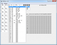
i4004 simulator
- Thread starter dwesti
- Start date
Dwight Elvey
Veteran Member
Next is to instrument your simulator to run some code. An interesting piece of real code is to implement Tom Pittman's resident assembler. It requires at least 3 4002s and resides in 1K of 4004 code. It uses a TTY serial input and output stream. This requires both RAM output ports and ROM input ports. It would normally run on a SIM4-01, SIM4-02 or SIM4-03. Description of a SIM4-01 can be found on bitsavers, MCS4 Users Manual.
Do note that this code depends on the proper 4004 stack operation. As a hint, the code will not run on a 4040 based machine. Tom also depends on the proper action of instructions like FIN and various, partial address, page fetching instructions to do the right thing on page boundaries.
The TTY assumes a ASR33 running at 110 baud. It assumes that the source is on punch tape and it writes out the first pass and final binary on the punch tape. The binary is in BPNF format as described in the manual for submitted ROM images( also in data bit inversed as would be used be used, with a SIM4-01 and MP7-03, 1702A, programming setup ).
I believe, if your simulator can properly run Tom's assembler, it is likely to be able to simulate any 4004 code.
Dwight
Dwight Elvey
Veteran Member
The 4040 can nest 7 levels before overflowing, while the 4004 can only nest 3 levels before overflowing. Tom's code depends on the proper behavior on an overflow.
Dwight
Dwight
Dwight Elvey
Veteran Member
Not all the ones on the web will work right. There are 4 registers pointed to by the current PC. As is normal, the the next sequential address is place in that register pointed to by the current PC, the called address is place in the next register and the current PC point uses that new register.
When the stack is over written and followed by code that does 4 BBL instructions, on the 4th BBL return, it will go to the address that was over written by the JMS call.
Tom uses this to change the flow of the state of the program. Since the 4th JMS doesn't overwrite the return address on a 4040, the code, as written will not work on the 4040. Almost no one uses this difference between the two processors that I've seen. You have to remember, Tom wrote the assembler to fit into 1K of code space. He used just about every possible trick.
There is one other funny behavior that I've seen used for both the 4004 and the 4040. The JCN has 8 possible actions based on the condition code. One of those is an "Always" jump that is redundant with the JUN but only on the same page. This is one of the funny page based difference if the code is at a page boundary. There is no advantage to using this instead of the JUN but a simulator must still do the right thing. The other rarely used variant is the "Never" jump. This is a tricky one. When I disassemble this one, I always use the additional instruction of SKIP to make the code more readable in the disassembly. The skipped address is often used for a single byte instruction, like LDM. This is often used at the beginning of a subroutine. This allows the subroutine to start with multiple possible values in the accumulator. The code might look like:
ENTER1 LDM 5
SKIP
ENTER2 LDM 4
... do something with ACC
BBL 0
This allows the same subroutine to be used from multiple places that require 4 in some cases and 5 in others. It only makes sense if you have multiple times you need these different values, otherwise it one would use the LDM instruction before the call. I've seen this used in code that was used to run a printer.
I hope this helps you get you simulator working correctly.
You should probably make a input option for you simulator that would take either binary or BNPF code, with the option to use bit inversion. That way it could use Tom's assembler to create code to simulate.
Making a simple way to instrument the assembler with I/O operations would enhance its use. Things like buttons for inputs and lights for outputs would be useful. Also adding the ability to add things that can be que'd up like serial data I/O, that is cycle count determined, would be useful, especially for something like Tom's code.
You'd then have something that would be off more use than just executing a string of instructions.
Dwight
Yes, I was confused by the description of the stack, and many emulators use a different implementation of the stack
Yea, there's nothing more fun than testing your simulator against one a "working one" that just happens to be wrong.
Yea, there's nothing more fun than testing your simulator against one a "working one" that just happens to be wrong.
I don't understand your sarcasm
Dwight Elvey
Veteran Member
One of the emulators' errors is the DAC code
I believe that the carry flag is defined incorrectlyCode:void dac() { rega--; if (rega & ~15) fcarry = 1; else fcarry = 0; rega = rega & 15; } /* dac */
It is not clear what the size of reg is in bits but assuming it is at lest a byte size,
only 0 should should not set a carry. All other numbers, 1 to 15, inclusive, should create a carry.
I would say the code fails.
Dwight
Al Kossow
Documentation Wizard
Dwight Elvey
Veteran Member
Hi Al
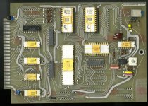
I don't recognize it. It is clearly a controller card for something. It might be a version of one of the Prolog 4040 boards but I don't think so. Sometimes a dump of the EPROMs will give some indication. I decoded some EPROMs for a friend that had a Prolog 4004 board. It was clearly use as a printer control. I forget which but one of the printer companies used the Prolog boards.
I'd suspect the DM8898 is used for input? It might be something like a BCD thumb wheel switch or something, assuming it is wired as an input. The wiring configuration might give a clue. The 3404s are output latches. It was likely made in a narrow range of time. The 4289 and the 4201 together were only made for a short time. the 4201 was soon replaced by the 4201A and the 4289 replaced the 4008/9 chipset.
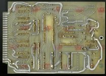
I'd be curious to see the backside wring?
Dwight
Al Kossow
Documentation Wizard
Dwight Elvey
Veteran Member
Oops,
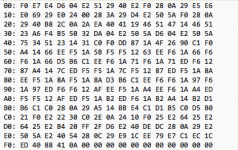
Each EPROM is 256 bytes. There are two EPROM that would be 512 bytes. Your listing is only 256 bytes. I've not looked at the wiring but I expect all 8 address bits are connected to each EPROM
Thanks for the picture.
Oops, I see the one EPROM is dead. Such it life. Sorry about that.
Dwight
Each EPROM is 256 bytes. There are two EPROM that would be 512 bytes. Your listing is only 256 bytes. I've not looked at the wiring but I expect all 8 address bits are connected to each EPROM
Thanks for the picture.
Oops, I see the one EPROM is dead. Such it life. Sorry about that.
Dwight
Last edited:


