• Please review our updated Terms and Rules here

Mostek/Fairchild F8 Evaluation Kit board, looking for pinout diagram

1944GPW

Veteran Member
Joined
Apr 26, 2011
Messages
809
Location
Brisbane, Australia
Well this is my first rather long-winded post here on what looks like a terrific forum.

Way back in 1978 my dad (an IBM engineer) thought that as kids, my brother and I would have a lot of fun and gain a better understanding of computers if we had our own. Very few kids had a 'home computer' in Australia back then, so naturally we were pretty excited. A work colleague of dad's who was a hardware guru had a working F8 system so we duly bought the same, known as the 'Mostek/Fairchild F8 Evaulation Kit / Design Kit'. It had 1k of RAM and 1k of ROM (containing the FAIRBUG monitor) and an unconventional CPU spread across three 40-pin DIPs.

When it arrived I guess my brother and I were expecting something that we could put a screen and keyboard on, and run BASIC, but what we got was a kit board and a bunch of chips. Dad had some junked IBM parts such as a 3277 EBCDIC keyboard, a Selectric I/O Writer (with the solenoids under the unit) and some 8" floppy drives. That was going to be our I/O and storage. Dad's hardware guru friend had designed and built the Selectric interface, as well as the converter for an IBM 8" floppy drive to a microcomputer, so we were going to build the same.

After soldering the board together we made a box and +5v/+12v power supply, but that was as far as we got. We spent some time learning F8 assembly and Dad wrote a program and designed a circuit to map EBCDIC to ASCII, and contemplating wire-wrapping a 4K or 8K memory expansion board using 2102's.

Time passed and not much later the F8 was put aside in favour of a lot more capable Applied Technology S-100 system kit with ASCII keyboard and a REAL VDU SCREEN!
Dad was a little disappointed that we never finished the F8 but we made up for it spending a lot of time playing about and learning on that machine and all the following ones but that's another story. So in the end, we never actually got to the stage of even powering up the F8.

Fast forward 30+ years and a few moves, and I thought that I'd have a go at trying to get the F8 to work, not just for my sake but in memory of my Dad who was always keen to help and support us learning about technology. Sadly the Selectric I/O typewriter, 3270 keyboard, floppy drives and other parts have been lost over the decades, all I have left is the original cardboard carton the F8 arrived in.

So... I unpack the dusty box and check that everything's still there. Assembled board and edge connector, check. F8 Data and Programming Guide books, check. Some advertising, check. Microcomputer-to-Selectric I/O interface circuit diagram (all 8 pages!) check. Some EBCDIC mapping code, check. Tiny BASIC article from Dr Dobbs, check. You can see this in the attached photos.

But.. the F8 Evaluation Kit board assembly diagram with the edge connector pinouts... missing! And I think there was a booklet on using FAIRBUG that's gone too. (I found another posting here on exactly the same board as I have but the poster isn't active, see http://www.vintage-computer.com/vcforum/showthread.php?16755-Fairchild-F-8-SBC)

It's probably a longshot but if anyone has the board edge connector pinout and FAIRBUG command guide I would be extremely grateful!

Steve.
 

Attachments

  • F8_kit_1.jpg
    F8_kit_1.jpg
    81.8 KB · Views: 6
  • F8_kit_2.jpg
    F8_kit_2.jpg
    57.7 KB · Views: 6
Last edited:
Chuck,
That..... is..... incredible! That's it!!!!! That's the circuit diagram I remember, and the pinouts I need, and the FAIRBUG manual, and a whole bunch of other stuff too! Ah, it's mindboggling thinking about the power of the Internet and a forum like this, and bitsavers.
Thank you again Chuck for your _amazingly_ fast response, I am really really grateful! :) :)

Steve
 
I've got the FAIR-BUG (KD-BUG) User's Guide and the F8 & F3870 Guide to Programming (which I gather you have) and I think I may even have one or two of the other cards; I don't think I have any documentation on the Evaluation Kit, but I'll keep my eyes open.

Edit: I was going to suggest that Chuck might be able to help, but I see that he beat me to it while I was typing; I'll have to learn to type faster ;-)
 
Chuck,
That..... is..... incredible! That's it!!!!! That's the circuit diagram I remember, and the pinouts I need, and the FAIRBUG manual, and a whole bunch of other stuff too! Ah, it's mindboggling thinking about the power of the Internet and a forum like this, and bitsavers.
Thank you again Chuck for your _amazingly_ fast response, I am really really grateful! :) :)

My pleasure, but you can thank Al Kossow for putting together the bitsavers collection. AFAIK, it has the only real information on the Fairchild Sentry CPU used in F's ATE gear anywhere on the net.
 
Thank you too Mike, it's good to know that this information is still out there. Yes I have the Guide to F3850 Programming. I can see that the F3870 was a perfectly logical decision to incorporate the separate CPU parts into a single DIP. I'd be interested in seeing a photo of your other cards, if it's not too much trouble? And I could get around to scanning the I/O Selectric interface circuit if anyone was still interested.

Steve
 
I'd be interested in seeing a photo of your other cards, if it's not too much trouble? And I could get around to scanning the I/O Selectric interface circuit if anyone was still interested.

Steve
I only think I've got a card or two like that; they have an unusual form factor and I seem to remember that a place I worked at long ago was making accessory cards for the F8 Eval kit. If I run across them I'll let you know, but don't hold your breath ;-)

As it happens I think I also just saw the book "Interfacing the I/O Selectric" somewhere in the chaos here a few days ago...
 
F3870 Guide to Programming

F3870 Guide to Programming

I've got the FAIR-BUG (KD-BUG) User's Guide and the F8 & F3870 Guide to Programming (which I gather you have) and I think I may even have one or two of the other cards; I don't think I have any documentation on the Evaluation Kit, but I'll keep my eyes open.

Edit: I was going to suggest that Chuck might be able to help, but I see that he beat me to it while I was typing; I'll have to learn to type faster ;-)

Anyone - I have been looking for the F3870 Guide to Programming for several months is there any chance that someone could send me a copy?
 
Last edited:
In case Eller ever comes back, the F8 Guide to Programming wasn't recycled and should appear on Bitsavers some time soon.
 
In case Eller ever comes back, the F8 Guide to Programming wasn't recycled and should appear on Bitsavers some time soon.
Is it there now? I'm interested in reading it. Thanks in advance.
 
Is it there now? I'm interested in reading it. Thanks in advance.
Apparently not; I sent two copies and some related stuff to a fellow hobbyist on the understanding that he was going to scan it and pass it on to Al at Bitsavers, but of course time is always in short supply. I'll check with him to see how it's going.
 
I haven't posted anything on my progress for quite some time, but seeing as how my thread has bubbled back up with someone else's request for F8 info, this is where I'm at with the F8.

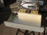
Needing a chassis for the board, I used a small 19" rackmount box and panel from a discarded modem. It didn't have a rear panel so I made one from a piece of sheetmetal, and fitted the IEC mains socket and fuse to it:
F8 chassis.jpg

The modem circuit board had a +5v regulator on one corner of the circuit board. I hacksawed this section out of the board and was going to use it but since I needed a +12/+5 v supply I ended up making one up from a salvaged 7812 and 7805 on a piece of Veroboard, and used connectors from an old PC power supply. The debug and reset switches were also from an old PC case.

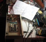
I wired it up for what I thought was the EIA (RS232) interface according to the circuit diagram from bitsavers, and hooked it up to an USB to serial converter and attempted connection at 110 and 300 baud, but after mucking around with it for some time I got nothing at all echoed back to the terminal program. I don't have an oscilloscope so for allI know the board may not even be generating a system clock pulse from the simple RC circuit. I adjusted the trimmer but that didn't help:
F8 first test.jpg

That's where I left it. However, not long ago I happened to find the missing manual for the F8 board, which was not on bitsavers. It's the VERAS SYSTEMS F8 kit manual and amongst other things has the component layout and most importantly, the modifications needed (ie. traces to cut and join) to use it with RS232. I haven't done those yet, but will do so and see what I get. The VERAS board is as far as I can determine identical to the original Fairchild board.

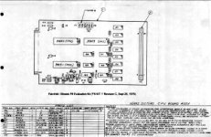
I've scanned this manual and need to turn the 20-odd pages into a PDF, and then submit it to bitsavers if they want it. It has the circuit diagram, board layout (below), component list and how to use FAIRBUG and some paper tape images:
F8 KIT 1 VERAS SYSTEMS CPU BOARD ASSY reduced.jpg

Looking through old issues of BYTE it seems VERAS made a complete turnkey system, with memory upgrades and a small software offering.


Steve.
 
Hi
Has anyone disassembled the code on the Video Brain.
I've alway meant to do it on the box I have but
just never seemed to get around to it.
Dwight
 
Apparently not; I sent two copies and some related stuff to a fellow hobbyist on the understanding that he was going to scan it and pass it on to Al at Bitsavers, but of course time is always in short supply. I'll check with him to see how it's going.
Thanks. Anything related to the F8 that's not already up there is appreciated.
 
I haven't posted anything on my progress for quite some time, but seeing as how my thread has bubbled back up with someone else's request for F8 info, this is where I'm at with the F8.

Needing a chassis for the board, I used a small 19" rackmount box and panel from a discarded modem. It didn't have a rear panel so I made one from a piece of sheetmetal, and fitted the IEC mains socket and fuse to it:
View attachment 8988Steve.
Very nice! Gonna put some blinkenlights into those holes?

That board looks so damn familiar; I've either got one somewhere or at least I had one at one time, which would explain why I had the manuals... Just curious: what are the dimensions of the board?
 
Mike,
Some blinkenlights would be nice I agree. The holes in the panel are from the modem status LEDs but there are not enough of them and they are asthetically in the wrong position. I used two of the holes to poke the debug and reset switches through. I have thought about how a front panel might be done - on bitsavers I found a manual for an S100 front panel (the Wameco FPB front panel board) and also the front panel schematic for the PDP-11/05 in the engineering drawings print set, and they appear to be a good starting point for a panel design.
However, nice as that would be, I have other projects to tackle (two PDP-11/05's) that I'd like to get on to.

By the way, the F8 board is 230 mm long x 130 mm wide (9.05" x 5.12" imperial). I have finished scanning the assembly instructions for the board and made them into a 22-page PDF (by pasting in the JPEGs into an OpenOffice document and exporting as PDF) but it's about 26Mb at the moment so I will reduce the image quality or size and try again. If possible I would like a copy of the manuals you mentioned you had for someone else?

Steve.
 
Hi
You might find making a front panel on a small developement
board. In order to work, the front panel board must take over
the bus and block data going to the processor. It must also be able
to halt the processor.
The bus on a S100 has 3state buffers that can be turned on
or off to isolate the processor.
Generally, the front panel also takes advantage of using the
processor to hold the address. As with the 8080 or Z80, it
forces the jump instruction onto the processor so that the
processor can write the address to the bus. This is what is
typically done to do the examine. The next is just forcing
a nop into the processor to advance the procssors address.
This is all difficult to do without bus buffers to separate the
processor from the RAM and ROM. Typically these smaller
boards directly drive the data bus.
Dwight
 
If possible I would like a copy of the manuals you mentioned you had for someone else?
I found them here. Thanks to Sean Riddle for posting them.

F8 info
more F8 info
3850 CPU data sheet
3851/3856 PSU data sheet
3852/3853 memory interface data sheet
F8 Guide To Programming
F8 family datasheet
F8 chapter from uP Terry Polhoff 1979 programming book

I also have found tools and code mostly related to programming games for the Fairchild VES (game system). The VES has an F8. I've attached some of it. The Pacman attachments are the source code for the excellent port of the game to the VES. (I had to split the files into two folders because of the attachment size limitation. Take the file out of the second folder and put it with the rest.)
 

Attachments

  • VES-Disassembly-Bios.asm.zip
    11 KB · Views: 3
  • VES-Disassembly-Videocart_26.asm.zip
    23.5 KB · Views: 3
  • pacman_pt2.zip
    92.1 KB · Views: 3
  • pacman.zip
    46.2 KB · Views: 3
  • F8_instruction_set_table.doc.zip
    12.8 KB · Views: 3
Back
Top