rmay635703
Veteran Member
My old IBM 5170 has sat missing 1 piggyback chip for a long time and has 2 others dislodged.
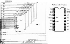
I am curious if I can substitute Siemens 41256-12's in my old AT mobo.
I am uncertain if the pinouts are the same as the old TI ZA1250Nls aren't spec'd anywhere.
I have a feeling that if the address pins, voltage and ground end up where they are supposed to be the board should use the chips but won't see them at full capacity, probably half.
Any ideas?
Also on an off topic this board appears to have 2 standard BIOS chips and one of the old window type chips, IS the AT board one of those that would tolerate a bios from a more modern AT board?
I have a 1989 AMI 286 bios plus in the old ODD EVEN 2 chip format that looks like it would fit right in, unless those are for basica.
I really don't know much about the true blue AT, like I do for the PC/XT's
Thanx
Ryan
http://www.vintage-computer.com/vcforum/newthread.php?do=newthread&f=22

