• Please review our updated Terms and Rules here

VGA Card Circuit Diagram for GD-5420

mmruzek

Experienced Member
Joined
Sep 28, 2011
Messages
227
Location
Michigan, USA
Hello, I have been exploring options for creating a VGA card for the PC-Retro from scratch and there is alot of terrific information available from the S-100 guys and Sergey. (Thanks!) I just happened to come across this manual for a Winsystems VGA card that not only includes a parts list, it also has the circuit schematic. I don't know if this is already well known and out there, but this is the first time I've seen it... so here is a link to the PDF for reference.

http://www.winsystems.com/manuals/LPMMCM-SVGA.pdf

Michael
 
I just happened to come across this manual for a Winsystems VGA card that not only includes a parts list, it also has the circuit schematic.

I think S-100 guys design is based on that schematic. The only problem (or rather an uncertainty) is why they are using MD0-MD15 lines... According to Cirrus Logic datasheets and manual these signals are not implemented on CL-GD5420. If it is true, it makes a half of the video memory useless.

If I am not mistaken the maximal memory supported by CL-GD5420 is 1 MiB in 512 K x 16 configuration (usually implemented using a couple of 512 K x 8 DRAMs), while other CL-GD542x controllers can use 256 K x 32 configuration (usually implemented using eight 256 K x 4 DRAMs, or on newer cards using a couple of 256 K x 16 DRAMs). This provides twice the memory bandwidth - 32 bit channel instead of 16 bit.

But it is possible that later revisions of CL-GD5420 supported 32 bit memory... not sure.

It looks like I am getting closer to the end of my previous project (ISA FDC card and the related BIOS extension). And if nothing else happens an ISA VGA controller will be my next project.
 
Hi
Yes, the Winsystems schematic was a reference guide but not the only source of information. The S-100 VGA and its ISA VGA prototype both use the 32 bit RAM access. The ISA VGA does work and has taught us quite a bit about why the S-100 VGA is not working. I suspect the real insight though is how the ISA VGA works on the 8 bit ISA and we'll end up using something like that to fix the S-100 VGA. As it is now, it is a pure 16 bit board and the differences between ISA-16 and S-100 16 bit accesses appear to be the root problem.

I think the ISA VGA design could easily be modified for a board on its own. We used it as a prototype to debug the S-100 VGA but that wouldn't stop it from being useful on the ISA bus. I think a lot of debugging components would just come off altogether. You are free to use the ISA VGA information we have on the N8VEM wiki including all the KiCAD EDA files.

Thanks and have a nice day!

Andrew Lynch
 
I did some research and it looks like the revision B of CL-GD5420 (part name: CL-GD5420-75QC-B) does support 32-bit memory interface. Likely the following revisions (e.g. rev. C) also support it.

And so it seems that eight 256 Kbit x 4 DRAM chips is the most flexible configuration supporting from 256 KB (two chips) to 1 MB (8 chips). These chips are also cheaply available (about $2.5 / each).

I hope to have an initial ISA SVGA schematic version later this week.
 
I hope to have an initial ISA SVGA schematic version later this week.

Well, it took me a bit longer. The schematic is here:
http://www.malinov.com/Home/sergeys-projects/isa-supervga

I changed my mind regarding the SVGA chip, and this design uses Trident TVGA8900i IC.
The reasons for this decision are:
- Trident TVGA8900i is a known 8-bit friendly chip. CL-GD542x might work with 8-bit bus, but it is not completely clear if it will work with latched address lines (SA17-SA19 instead of LA17-LA19).
- Trident's BIOS uses only 8088 instructions, while Cirrus Logic uses some 186+ instructions, and I don't feel like disassembling the BIOS and modifying it to use only 8088 instructions.
- If I remember correctly Trident was very good with emulating older video cards (CGA, Hercules).
- It looks like Utsource has more TVGA8900I-1(-2,-3) ICs in stock than CL-GD5420. Other suppliers seem to have it too.

Current schematic is based on JA-8237A/V2 card (minus 16-bit ISA part). Please let me know if you happen to have a TVGA8900i card, as I want to verify values of a few capacitors.

Thanks,
Sergey
 
Sergey, This is terrific! I have been trying to source the CL-GD542X video chips in larger quantity for the PC-Retro project and was only able to find them at UT source for about $15 each, as you mention. Also, I completely agree with the desire to avoid disassembly and modification of the video BIOS for the Cirrus Logic chip.

Also, I will look in my VGA card collection to see what I have from Trident. Looking at a photo on EBAY it appears this video board uses mostly surface mount components.
 
Last edited:
Looking at a photo on EBAY it appears this video board uses mostly surface mount components.

That was exactly my problem. I was able to reconstruct the schematic looking at the board and at the TVGA9000i datasheet, except of SMT capacitors, that don't have values printed on them. Fortunately yesterday I picked up another TVGA9000i card at the local surplus store (nice place, BTW), that uses through hole components.

I am working on the PCB layout now, depending on the available time it might take anything from a few days to a week or two. :)
In parallel we can check prices and availability of TVGA9000i (I think TVGA9000I-3 was the latest, with some bugs fixed).

Once PCB layout is finished I'll order 3 (or so) prototype boards from OSH Park, and hopefully test the design :)
 
Update: The PCB layout is mostly ready. I uploaded the printout (PDF) of the current version to the project's page. See attachments / version 0.6.

TODO:
- Add some vias between GND zones
- Arrange components' reference and value labels on the silkscreen
 
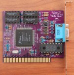
I received the prototype PCBs for my ISA Super VGA board, and built one of them yesterday.

ISA SVGA - Board.jpg

Soldering the 160-pin flat pack Trident TVGA9000I chip was simpler than I expected. After carefully positioning the IC, and soldering a couple of pins on the corners, I just had to use thin (0.015") solder, and some solder wick to remove occasional solder bridges.

The card runs nicely with either 256 KiB (2 DRAM chips) or 512 KiB (4 DRAM chips). And it works without any problems in my Xi 8088 system with ISA bus clocked at 13.3 MHz.

I have a minor layout issue with EMI filters - they have bigger diameter than I expected (about 3 mm instead of 2.5mm?!), so they interfere a bit one with another, but it shouldn't be too difficult to fix for the production version. BTW, I don't think these filters are essential for the card operation, they intended to reduce the EMI the card generates (apparently to meet FCC requirements).

More high resolution pictures here: https://picasaweb.google.com/skiselev/ISASVGA.
Project page is here: http://www.malinov.com/Home/sergeys-projects/isa-supervga. The page is a bit outdated, I will update it with BoM and other information soon.
 
That looks very nice, Sergey. I'm looking forward to buying one (or two). It'll be a great addition to my in-progress Xi 8088.

Looks like I may need to invest in a bigger magnifying lens and a teeny-tiny soldering tip before tackling that 160-pin flat pack .

<*> Jim
 
Back
Top