• Please review our updated Terms and Rules here

CGA card with burned trace

FiveGHz

Member
Joined
Sep 3, 2019
Messages
19
Location
Cambridge, MA
Hi all, I recently came across an IBM 5150 on the side of the road in pretty decent condition. I took it apart to inspect the components before powering it up, and I found a burnt trace on the CGA card. I used a multi-meter to test for continuity, and the trace definitely is cut. It seems to be connected to one or two of the actual pins on the connection to the monitor. I don’t have a lot of experience with this stuff, but was wondering if it would be safe to just add a jumper wire around the cut, or if there is something else I should be concerned about.
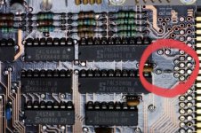
C00173D7-7DC7-483A-9B4C-50AA90646C5E.jpg

Any insight is appreciated.

Thank you.
 
I see that the trace appears to be B9, the +12V line. So where does that go? Well, the schematic says that it goes to the 4 pin Berg connector (P1) for composite video out and also to P2, the 6-pin light pen connector. So, if you're connected to the DA-9F J2 connector and not using a light pen, you've no need of the +12 line.

So where might it have come to grief? Well there's a 10 uF tantalum on that line--it's probably what caused the blown trace. Replace the tant and fix the trace with a bit of wire and solder. I repair traces with AWG30 wire-wrap wire, but you can use whatever you've got.

Hi Chuck(G),

I’ve found the logic diagrams in the IBM CGA card’s manual but can’t seem to find the circuit diagram. If you could help point me in the right direction it would be most appreciated. Googling IBM CGA schematics or circuit diagram doesn’t seem to turn up what I’m looking for :)

The board number on my card is 6133807. On closer inspection, it appears the tantalum cap on C8 might be blown.
 
Thanks Chuck(G), on closer inspection it does appear that the capacitor on C8 is damaged. I’ll replace that and the trace and see if it works.

Just curious where you found the circuit diagram. I see the logic diagrams in the CGA card manual but no schematic for the circuit.
 
Thanks and sorry for the double post. It took a while for it to get approved and I thought it may not have gone through.
 
Back
Top