• Please review our updated Terms and Rules here

Yup, another IBM 5160 failed motherboard

tonata

Experienced Member
Joined
Sep 11, 2019
Messages
190
Location
France
I have a 5160 XT 64-256 motherboard.

Last time I tried to swap the CPU with NEC 12 Mhz one and it did not work. So I tried the original one and it still did not work. Motherboard appear "dead".

Procedures done so far:
- minimum diagnostics setup does not work.
- the CPU is OK, I tried it on another motherboard.
- I checked the 40 pins of the CPU socket for connection with the other side of the motherboard - all connected. A bad socket or a damaged one could explain everything.
- POWER is OK. I powered another motherboard with the same power supply. Voltages are OK.
- I changed capacitors: C58, C59, C56, C54, C68. Middle pin is +, outside is -. Longer leg of the capacitor is + (there is a + also on it)
- I re-socketed the entire 9 x 4 = 36 memory chips
- I exchanged the memory chips from BANK0 and BANK1

What else can be done ? :)

I have a hard time identifying the memory chips.
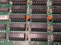
IMG_20201122_212018.png
 
Last edited:
Last time I tried to swap the CPU with NEC 12 Mhz one and it did not work. So I tried the original one and it still did not work. Motherboard appear "dead".
So, the motherboard was working before you put in the NEC V20 CPU ?

- POWER is OK. I powered another motherboard with the same power supply. Voltages are OK.
So, on the faulty motherboard, the voltages and POWER GOOD signal are good (per [here]) ?

What else can be done ?
Do you have a Supersoft/Landmark Diagnostic ROM ?
If so, does it show anything ?

If not, do you have another BIOS ROM chip to try ?

Per [here], do you have the means to see if the CPU and 8288 chip are getting a 4.77 MHz clock signal ?
 
I have a hard time identifying the memory chips.
Based on the symbol, the chip maker is Siemens (see [here]).
A search for "Siemens 8493286" shows some hits, some including "DIP16", and so I suspect that 8493286 is the part number.

Siemens' normal chip for ths application is the HYB4164. Maybe IBM had Siemens label their HYB4164 as the IBM part number of 8493286 ?
And IBM may have had other makers do the same thing, e.g. "intel 8493286" appears at [here].
"8493286" also appears on these forums at [here].
 
Yes. It was working. But then I did not test immediately before changing the CPU. So 10 days before changing the CPU was working.

Yes I checked the voltages per here

I do not have EPROM writer or Diagnostics ROM. I have ROMs from another IBM 5160, but still they are not diagnostic.

I have a logic probe and multimeter. Maybe I can access another equipment if I know exactly what I need to see the clock signal.

So, the motherboard was working before you put in the NEC V20 CPU ?


So, on the faulty motherboard, the voltages and POWER GOOD signal are good (per [here]) ?


Do you have a Supersoft/Landmark Diagnostic ROM ?
If so, does it show anything ?

If not, do you have another BIOS ROM chip to try ?

Per [here], do you have the means to see if the CPU and 8288 chip are getting a 4.77 MHz clock signal ?
 
Last edited:
I have ROMs from another IBM 5160, but still they are not diagnostic.
A faulty BIOS ROM is a possibility, so try a BIOS ROM from another 5160.

I have a logic probe and multimeter. Maybe I can access another equipment if I know exactly what I need to see the clock signal.
Your logic probe should show alternating signals, such as clocks.
Use it to see how it behaves when measuring the 4.77 MHz clock on your good 5160 motherboard.
It will not tell you the frequency, but it will give you confidence that the clock is present.
 
So the 8288 is next to the power supply and the FPU. It is U8.
In your link link it is 8284A. It is not 8288, bit I suppose it is OK.
So pin 2 of the 8288 gives clock on the probe.
Pin 19 on the CPU gives clock also.
 
So the 8288 is next to the power supply and the FPU. It is U8.
In your link link it is 8284A. It is not 8288, bit I suppose it is OK.
The link shows the 8284A generating the 4.77 MHz clock, with the "CPU, 8288, NPU" receiving that clock.

(The NPU {8087} socket does not need to be checked. The NPU, if present, is not involved in the starting of the 5160.)

So pin 2 of the 8288 gives clock on the probe.
Pin 19 on the CPU gives clock also.
Giving you good confidence about the 4.77 MHz clock.

Refer to [here]. Does your logic probe show pulses on pin 13 of the 8253 chip. If it does, it means that the POST has started (reaching at least step 13 at [here]).

Tried another set of IBM BIOS ROM's ?
 
I checked with the other ROM chips. It did not work. But then these other ROM chips are from upgraded MB from 16-256 to 256-640 by IBM. So it is another version of the ROMs 1986 compared to 1983 (the failed one) and this upgraded MB has some extra cables around the ROM chips. So I am not sure it was compatible?

Pin 13 gives red 5 V, instead of pulses. So definitely a problem?

Can I check if the CPU is halted?
 
Last edited:
PB7 on 8255 shows no state. The logic probe diodes are all dark.
It is supposed to be high?

And when I say that there is "clock" actually 3 diodes are on: red, orange (pulse) and green. It is not just blinking the orange one (pulse). Maybe when the frequency is too high is like that. It is the 3 instead of a pulsing orange diode.
 
Last edited:
Pin 13 gives red 5 V, instead of pulses. So definitely a problem?
It is informing you that either:
* The POST is not starting, or
* The POST is starting, but not getting as far as step 13.

Can I check if the CPU is halted?
Yes, but that will not inform you of what caused the halt, or when the halt occurred.

I checked with the other ROM chips. It did not work. But then these other ROM chips are from upgraded MB from 16-256 to 256-640 by IBM. So it is another version of the ROMs 1986 compared to 1983 (the failed one) and this upgraded MB has some extra cables around the ROM chips. So I am not sure it was compatible?
The "extra cables" on your 'upgraded' 256-640KB board will be IBM's rewiring to accommodate 27256 type ROM's. Some photos in links at the bottom of [here].

The 05/09/86 BIOS on a 64-256KB motherboard should, at the least, start and display something. I will put the 05/09/86 BIOS into my 64-256KB motherboard, and report back.

PB7 on 8255 shows no state. The logic probe diodes are all dark.
It is supposed to be high?
At power-on time, PB7 will be an input. Per step 5 of [here], the POST configures the pin as an output. So your measurement indicates that if (and if) the POST is running, it is not getting as far as step 5.

And when I say that there is "clock" actually 3 diodes are on: red, orange (pulse) and green. It is not just blinking the orange one (pulse). Maybe when the frequency is too high is like that. It is the 3 instead of a pulsing orange diode.
The manual for your logic probe will tell you what it displays for different things.
 
Thanks!

The 3 pins 26,27,28 S0,S1,S2 are all high. So this is a HOLD state. Here it is called "passive" and it means "No Bus Cycle".
Ready pin is HIGH.

In the past there was some suspicious behavior of 8255A, but it still worked OK. Could this be explained by a defective IO chip 8255A?

Maybe I can measure the clocks with oscilloscope of the other chips and rule them out?
 
The 05/09/86 BIOS on a 64-256KB motherboard should, at the least, start and display something. I will put the 05/09/86 BIOS into my 64-256KB motherboard, and report back.
I did that, and as expected, I saw a RAM count-up on the screen. So you can rule out a faulty BIOS ROM chip as the problem cause.

In the past there was some suspicious behavior of 8255A, but it still worked OK. Could this be explained by a defective IO chip 8255A?
The 8255A would have to be faulty in a way that interferes with operation of the address or data buses. Quite a few chips can do that.

(The "suspicious behavior of 8255A" that you refer to will be what you observed during the time that we were fixing your 'keyboard port does not work' symptom. From memory, the 'suspicious behavior' was later explained by a detailed look at what the POST does with PB6 and PB7 under certain failure modes of the keyboard interface circuitry.)
 
For the IBM 5160, the sequence of events that occurs before the POST starts is shown at [here]. To verify that ALL of that is happening, you would need a range of different test equipment (and the knowledge of how to use them).
 
8284 pin 10 goes from high to low.
So I see that chips are taken out of "reset state". The CPU pin 21 is low. The 8255 pin 35 is low. U21 pin 8 is low.

So now I can check if the 8088 is sending to the 8288 'Read Data from Memory' which is S2,S1,S0 = 1,0,1

How to test U14/U16/U17 ?

I can check if /CE goes to LOW on U18 to see it the ROM chip was successfully accessed.
 
So now I can check if the 8088 is sending to the 8288 'Read Data from Memory' which is S2,S1,S0 = 1,0,1
A logic analyzer. Again, like any test equipment, you will need to gain the knowledge of how to use it. You have a functioning 5160 motherboard and so you can use that for learning, and to see what the logic analyzer is expected to show on your faulty 5160 motherboard.

How to test U14/U16/U17 ?
In the day, we used an 'in-circuit logic IC tester'. For example, to test a soldered-in 7403 chip, we informed the tester that:
* a 7403 chip was being tested; and
* which pins of the chip that the circuit tied HIGH; and
* which pins of the chip that the circuit tied LOW.
We then clipped the tester's IC clip onto the 7403 chip then ran the test. The test would last a second of so.

That in-circuit test of the 7403 could have be done manually, temporarily tying input pins HIGH and LOW as required to verify the operation of each of the 7403's four NAND gates. Time consuming, and I always worry about the fact that in tying an input pin to HIGH or LOW, somewhere on the circuit, the output of a TTL device is being tied HIGH or LOW; is there a possibility of damage? I have used the technique over the past, say, 10 years, (usually to simulate a failure, rather than as part of failure detection) and have not (yet) seen damage.

Sometimes when I am fault finding a 5150/5160 motherboard that does not appear to be starting the POST, a quick look using my logic probe will reveal some activity on the address and data buses. Let us assume a 5160 motherboard. As an example, on U16 (a 74LS244 quad driver), I see activity on the (joined) enable pins, activity on all gate input pins, but one of the output pins shows no activity. Being TTL circuitry, it is very unlikely that something connected to the output pin is causing the problem, and so I would replace U16 with new.

For a transceiver on the data bus, you may see activity on all expected pins, but the problem may be that for one or more gates, the transceiver is not driving in one direction. Use of a logic analyzer will pick that up.

On the motherboard shown at [here], not only were there faulty chips, but battery leakage had caused faulty vias as well.

I can check if /CE goes to LOW on U18 to see it the ROM chip was successfully accessed.
So, like the text written at [here], activity on the /CE pin only informs you that the address decoding logic is sometimes asserting U18's /CE pin.
Activity gives good confidence, but maybe the address decoding logic is faulty, only decoding some of U18's address space.
 
Here there is a very cheap logic analyzer: https://www.amazon.fr/AZDelivery-Logic-Analyser-compatible-version/dp/B01MUFRHQ2/ref=sr_1_1_sspa
It is rather popular.
With this one I can detect how each pin changes on every IC, right?
Only 8 channels. That is quite limiting.

Okay for for something like [this], where only 4 channels are needed (POWER GOOD, PA0, PA1, PA2).

But, for example, what if you wanted to monitor the addresses and data lines of the U18 ROM, to verify that the addresses in and the data out is as expected. U18 has 14 address pins and 8 data pins. So, at the least, 22 channels. Then if you plan to use POWER GOOD or RESET as the trigger, you will need another channel. You will need to monitor the /CE pin as well, so you can tell which addresses on the address bus are being used by U18, and on the data bus, the time slots that are expected to contain U18 output data.

And when looking at the output of the ROM, you need to cater for the 8088's 'prefetch' mechanism.

And for channel count, the requirement gets greater for 16-bit systems (more address and data pins). But, in some cases, there is at least one workaround for insufficient channel count. At [here], I am monitoring the address and data pins on the BIOS ROM's of an IBM 5170, but my logic analyser does not have enough channels to simultaneously monitor all address lines and all data lines and some other things. So, in one operation I monitored all address lines and half of the data lines, then in another operation, changed to monitoring the other half of the data lines, then I manually pieced together the information.
 
The logic probe sampling frequency is 2 MHz. That is not enough? I need like 10 MHz sampling frequency to capture data been transmitted at 4.77 MHz ?
 
Back
Top