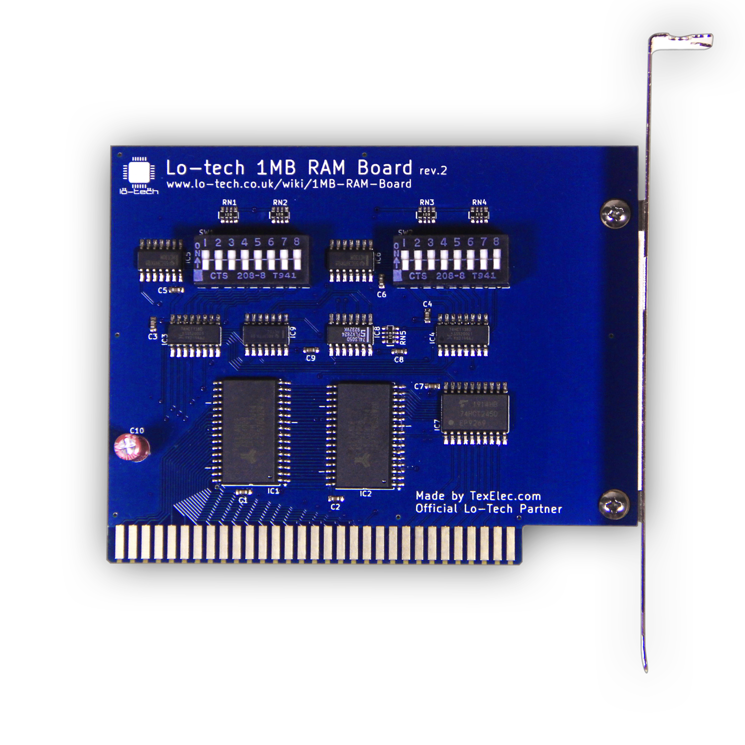
• Please review our updated Terms and Rules here

IBM 5170 restoration - PSU fixed, now RAM problems - SRAM replacement?

mrmanse

Member
Joined
Aug 19, 2015
Messages
44
Location
Borås, Sweden
Hi everyone!

If in a hurry, my questions are at the end.

So I bought an old 5170 a few years back at auction, with more or less unknown condition. I recently started working on the machine, which at first was dead, and quite badly corroded. The PSU was dead, but I located a failed LM324 circuit (IC0004), which fixed the problem. I made a schematic of the top PCB in the PSU, much like with the 5150 recently posted, but this one is needs some more work before ready for publication. If anyone should need it as is, just contact me.

Well, after I got the PSU working, the mobo was dead. I made BIOS replacement with two flash chips (29EE011 type) and put the Supersoft diagnostics on there. It ran quite unreliably, and never past the 16KB critical memory test. I replaced the corroded U27 and U47 IC sockets which at least made it run stably, but the memory issue remained. So I did the wiggle maneuver but with no luck. Unfortunately for me this was a type 1 motherboard with only 256KB on board, and I have no spare piggyback DRAMs. So I made a few suitable DRAMS by stacking some 4164 DRAMs (pins 1-3 needs some tweaking, but it's doable). Same result, seemed like many of the chips were bad and I couldn't identify which ones. I then got the idea of a complete memory replacement for the IBM 5170. Did a test with a 5V-tolerant 256kb x 16 dram laying around, and it kind of worked, at least partly. I got past the 16kB critical test, but it failed on the CPU protected mode (not the "normal" variant described by modem7, but the word Failed both on top of the screen AND in the column where it should say passed). It failed even worse with memory refresh tests, which isn't that surprising considering this was a completely different type of DRAM. So I started working on a SRAM replacement. It also isn't ready for publication, but I'll gladly share it in few weeks at most. It's based on 2 512kb x 8 SRAMs (yes, twice whats needed, but there are no 256kB x 8 :)). It worked better than the DRAM variant, and passed Supersoft memory testing up till 0x40000, where it failed on bits 0, 2 and 5. I've never had a 5170 before so it took me a while to realize that it was the 256/512kB jumper set in the wrong position. After correct jumpering the Supersoft passed ALL tests, from to to bottom - YEAH!

I then fixed a 6V battery (simply four 1,5V batteries in series), and set the correct settings in CBASIC using the GSETUP_BASIC app. Then troubles started.

1. The BIOS only identifies 384KB ram, both IBM 1984 BIOS and the AMI bios downloadable from minus zero degrees. This doesn't appear to be a configurable setting. I've tried to set it to 512KB, but I get the 203 error. Supersoft identifies and passes 512KB of RAM, but NOT if I a serial/parallell adapter is in ISA slot 2. I that card is in, Supersoft tests successfully up to 0x80000 (or 0x7FFFF) and then continues counting (and failing of course, even showing garbage on screen).
2. I have booted the machine to dos a few times, but it's unstable. I very soon get a parity error. So my plan is of course to get rid of the four remaining piggyback DRAMs used for parity and replacing them with parity calculating circuitry instead. There shouldn't ever be a parity error then, and with modern SRAMS on a enthusiast computer this safety isn't needed.

So - my questions - HOW exacly does the 5170 type 1 mobo identify the amount of onboard memory. Where did it get the 384KB from? Can it be set somehow that I've missed? I have checked and double checked my SRAM board, but since Supersoft finds all the RAM I don't think thats it.
Any other ideas would also be much appreciated.
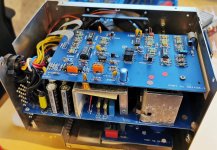
IMG_20201226_123149.jpg
Note the extra PCB with a quad OR gate. A required modification.
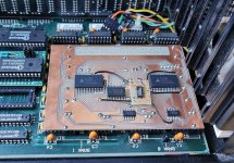
IMG_20210107_113041.jpg
 
1. The BIOS only identifies 384KB ram, both IBM 1984 BIOS and the AMI bios downloadable from minus zero degrees.
This doesn't appear to be a configurable setting.

If you are using IBM software, the author is probably assuming that only IBM options are used, e.g. for base memory, settings of 256K, 512K, and 640K.
I see that GSETUP.EXE has only 256K/512K/640K settings for base memory.
And I see that GSETUP_BASIC.EXE (I am the author) has only 256K/512K/640K settings for base memory.

384K is a very unusual conventional (base) memory amount to have in an IBM 5170.

So - my questions - HOW exacly does the 5170 type 1 mobo identify the amount of onboard memory. Where did it get the 384KB from?
The base memory figure that you set into the SETUP ('CMOS SETUP) is you informing the machine's POST as to how much base memory it should find at power-on.

The POST does a sizing check to validate that amount (e.g. has some base memory failed? e.g. has some base memory been added?). If there is a difference, a 164 error is displayed. The sizing technique used is the same as that used in the IBM 5160 - see [here].

Later, all of the base memory is tested (not just the first two bytes of each 64K block, as the sizing check does). A failure during this test results in a 201 error that points to the failing address.

I've tried to set it to 512KB, but I get the 203 error.
Hmm. A 203 error.

IBM's description of a 203 error is included at [here]. An address related problem.

but since Supersoft finds all the RAM I don't think thats it.

By that, I presume that the Supersoft diagnostic is successfully testing all RAM between the addresses of 0 and 512K.
Maybe the Supersoft diagnostic is not written to detect addressing problems.
 
The base memory figure that you set into the SETUP ('CMOS SETUP) is you informing the machine's POST as to how much base memory it should find at power-on.

The POST does a sizing check to validate that amount (e.g. has some base memory failed? e.g. has some base memory been added?). If there is a difference, a 164 error is displayed. The sizing technique used is the same as that used in the IBM 5160 - see [here].

Later, all of the base memory is tested (not just the first two bytes of each 64K block, as the sizing check does). A failure during this test results in a 201 error that points to the failing address.
Thanks modem7 for suggestion and reference! It makes sense and fits with my observations. I have programmed the value 512KB into CMOS, and verified that it sticks there. At power on the first memory sizing check counts to 512kB, but the second time to 384KB, and then gives a 203 message. I now understand better, maybe there is a problem with my SRAM memory board after all. Should be possible to detect with a logic analyzer. To be continued!
 
So, i think I got the SRAM replacement bord working (512KB SRAM. Still using piggyback DRAMS for parity in 9th column, but I'm waiting for parts to put a parity calculating hardware directly on the board and skip all DRAM for good). I have multiple full runs of Supersoft diagnostics without errors, I boot to DOS without errors, I run software from floppy without errors. But when I try to write something to the floppy, no matter what, the computer immediately hangs with "Parity Check 1" error. On second row five question marks are shown, no digits or other clues. This happens every time, with all floppy writes and immediately. Can't even do a "md test", format a diskette, "echo test > test.txt" or save a small file from Basic.com.

Is this a known problem? With the controller or so? with the disk drive? It would help a lot to get any details about the error, because if it isn't caused by the RAM i'd be very happy.

/M
 
512KB SRAM. Still using piggyback DRAMS for parity in 9th column, but I'm waiting for parts to put a parity calculating hardware directly on the board and skip all DRAM for good).
I am not following you. The parity calculating hardware (for motherboard RAM) is elsewhere on the motherboard with the piggyback DRAM's in the 'parity' column simply storing the output of the motherboard's parity calculating hardware. So all you should need to do to go fully SRAM is expand the data width of your custom board from two banks of 16-bit to two banks of 18-bit.

I have multiple full runs of Supersoft diagnostics without errors, ...
Which needs to be 'taken with a grain of salt'. We do not know how thorough it is.

... I run software from floppy without errors. But when I try to write something to the floppy, no matter what, the computer immediately hangs with "Parity Check 1" error. On second row five question marks are shown, no digits or other clues.
See [here]. So, a parity error in motherboard RAM, and the address at which the error occured could not be established.

... It would help a lot to get any details about the error, because if it isn't caused by the RAM i'd be very happy.
Parity error reporting is normally disabled during the POST, and so any parity error is normally either seen near the end of POST (when it is enabled), or later.

Any generated parity error happens during a RAM read operation, not a write operation. Even though you are writing to floppy, DOS and/or the BIOS could be reading RAM.

There can be many causes. For example, in the IBM PC, not having enough fitted RAM for the version of DOS being booted. For example, see the bottom right corner of [here].

Maybe one of those DRAM's in the parity column is faulty.
 
Again many thanks for useful feedback!

So all you should need to do to go fully SRAM is expand the data width of your custom board from two banks of 16-bit to two banks of 18-bit.
Yes, of course, but the memory I've chosen doesn't come in 9, 16 or 18 bit width, only 8. It's a 512Kb x 8 SRAMs, so I use two of them to replace the full 512KB of the motherboard. And since modern RAM is much safer, I've decided to fake parity in the board to get rid of the DRAM headache. I planning on putting two 74F280 on the board, feeding the computer a real-time calculated value based on the bits of the data pins. The 5170 will check the value with it's own 74F280's and hopefully be completely happy all the time, even if there actually was a RAM error. Most of us don't use ECC memory today and it works fine.

There can be many causes. [...cut...] Maybe one of those DRAM's in the parity column is faulty.
Yes, that seems very probable if the parity isn't tested either during POST nor with Supersoft. I must confess I thought the Supersoft diagnostics did a better better job.

I posted the question since the error was so very specific to floppy drive writing, that's all. But well, I have a couple 74HC280's here, they should be fast enough, so I'll give it a try tomorrow.
 
Maybe one of those DRAM's in the parity column is faulty.

Probably so. The SRAM board is now running with it's own parity generator, and it works well. No parity errors since this mod. The problem with writing on floppys still persist, though. Maybe it's ram related, maybe not, but I've made some observations that could be clues.

Configuration:
* 5170 type 1, 512KB SRAM
* IBM CGA adapter and original IBM MFM/Floppy adapter
* No other adaptors

The progress so far:
* System runs 100% stabily on floppies and passes Checkit 3.0 memory test, POST ram test, Supersoft diagnostics
* CMOS battery is now good, time is more or less correct, and there are no misconfigurations there.

The symptom:
* When writing to floppy, a whole sector of 512KB is overwritten with 0xFF. A good way of determining this is by changing a single byte in Norton Diskedit and updating the Sector.

These are things I've tried:
* different bioses (AMI bios, IBM 5170 1984 original BIOS), with same result.
* different floppy drives (two 5,25" 1.2M and one 3,5" 1.44M) with same result.
* different floppy controllers, different cables, and different drive letters (A/B) with same result.
* different DOS versions, different software for writing to the disk (DOS commands like md, rm, FORMAT.COM and such, Checkit, Norton Diskedit, and even the AMI bios built in diagnostics tools for formatting diskettes).

My own thoughts:
Since the system is continuing to run well AFTER the floppy writing error has occurred, I don't think there is a problem with system memory. At least in many ways it's working as it should. What I'm looking into is if something special is happening when writing to the ISA slot, and floppy controller. Could it be something like the Norton Diskedit buffer memory is overwritten when the 512B is supposed to be transferred to the controller? If it stores 512B data somewhere, and tries to read it and move it to the disk controller, losing the data in the process, it probably wouldn't affect overall system stability, I think. So if a WR line isn't working as it should? DMA related?

Any ideas appreciated!
 
To be honest, I don't think you get anywhere with your floppy issue without removing that SRAM expansion and try it with ordinary DRAM. I saw many people searching for such errors for weeks and months because they were sure "this certainly isn't the culprit".
 
I finally fixed it!!

I looked at the 82288 with my logic analyzer and realized that IOW and MEMR occurs simultaneously. So if MEMR and MEMW works well, but MEMR and IOW in combination doesn't there must be a timing issue with the SRAM board after all. Turns out there was. For CPU <-> MEM transfers, the SRAM chip select doesn't need to be active AFTER the rising of -RAS signal, but for MEM -> IO transfers to work, the SRAMs chip select needs to be active low as long as -CAS is active low. It works now. I'll write something up and post here.
 
Hi Mans,
this is an old thread, and I don't know, if you are still active here, but I give it a try:
I've got an IBM 5170 with failing piggyback ram on the mainboard. Since this type of ram is hard to find nowadays , I would like to replace it with an adapter board like the one you've build.
Would you mind providing a schematic for that board?
Thanks, Markus
 
It’s not that hard to find, if you broaden your search terms a little. I just go here:

And try a few different brands, etc, that show to be good, and then find a price I’m happy with:


Of course where you’re at on this planet may affect availability and prices. :)
 
It’s not that hard to find, if you broaden your search terms a little. I just go here:

And try a few different brands, etc, that show to be good, and then find a price I’m happy with:


Of course where you’re at on this planet may affect availability and prices. :)
Price is fine, but shipping costs to Germany are not :)...

Anyways, I'm more interested in building an adapter board as Mans did, than replacing the failing ram. This would be a good practice, too.
On the long run I expect more of this chips to fail, having a viable alternative on hand would be a goodie on top.
The builtin RAM extension card (the 128K version) is failing every now and then, too, but this is a different story...
I would be interested in something along this line as well. I am debugging a 5170 right now that has some bad memory, and that particular stacked RAM is getting harder to find. It would be reasonably straightforward to do a PCB ( I have done many )... We could start out by reaching out to Mans ( his email address is on that PCB picture ), to make sure we don't make any to the same mistakes he did.

As an aside - I'd have to look at the 5170 schematic, but it would seem possible to have the complete system memory on a 16 bit ISA card, and only have to make a small change to the PCB so the DRAM memory data buffers are not enabled when accessing the lower memory area. That should allow a card (that we make) in the ISA slot respond to lower system memory requests - And while we are there the same card could also provide extended memory.

Thoughts?
Since Mans obviously doesn't answer here, I also considered mailing him directly. To get a start and avoid some pitfalls, it's worth a try. Have you done that already?

The "ISA hack" sounds interesting, especially when capable as RAM expansion card too. But, when bypassing the onboard-mem, how does the CPU know where to find the appropriate address-space?
Is this achived by the small change to the pcb you mentioned? I would expect some boot-issues here, but to be honest, this is beyond my knowledge.

Rather than replacing all memory banks with one pcb, an alternative and perhaps simpler approach would be to just replace the failing stacked module(s) with a single board for each socket.
Besides the obvious memory wastage, are there any other objections to this?
A quick search here gave no result for a similar approach. I don't expect to be the first with this idea :) , so I'm wondering why this hasn't been discussed before. Can someone shed some light on this?

Thanks,
Markus
 
The "ISA hack" sounds interesting, especially when capable as RAM expansion card too. But, when bypassing the onboard-mem, how does the CPU know where to find the appropriate address-space? Is this achieved by the small change to the pcb you mentioned?
The CPU puts the address onto the address bus. It is up to RAM subsets (RAM plus supporting circuitry) on the motherboard and on expansion cards to monitor the address bus to detect when they are being addressed (and act accordingly for a read or write).

If the desire is to substitute for the 5170's motherboard RAM, i.e. addresses 0 to 512K, then:
1. Disable all of the 5170's motherboard RAM, which would require a mod ('hack') to the motherboard. See note 1 below.
2. Fit a 16-bit RAM expansion card that is configured for addresses 0 to 512K.

Note 1: On the IBM 5170 motherboard, removing RAM chips from a bank does not disable the bank.

Related to this discussion, the IBM 5170 motherboard has a jumper (see 'Jumper Block J18' at [here]) that can be used to disable the motherboard RAM that is in the address space of 256K to 512K. If that is done, a RAM expansion card, configured for addresses 256K to 512K could substitute for the J18-disabled motherboard RAM. IBM just didn't bother going one step further, a jumper position to disable all motherboard RAM.
 
Since Mans obviously doesn't answer here, I also considered mailing him directly. To get a start and avoid some pitfalls, it's worth a try. Have you done that already?

No, not yet, but happy to also reach out. I'll send you a DM and we can co-ordinate. It would be interesting to hear about a few of the decoding issues he had.
The "ISA hack" sounds interesting, especially when capable as RAM expansion card too. But, when bypassing the onboard-mem, how does the CPU know where to find the appropriate address-space?
Is this achived by the small change to the pcb you mentioned? I would expect some boot-issues here, but to be honest, this is beyond my knowledge.

Indeed, there is logic on the motherboard that decodes the requested address and enables the access to DRAM. In the case of the 5170, the address bus and data bus right off the CPU has a set of buffers, and past those buffers are the address and data lines on the ISA bus. Another set of buffers then connects to the DRAM and ROM (and there are a few other buffers in the mix for a few other things).
The key is finding the signal decode for the lower DRAM area and changing it so the buffers that connect to the DRAM to the databus such that it isn't enabled. This would allow memory that is on the ISA bus to respond to the access request.
Rather than replacing all memory banks with one pcb, an alternative and perhaps simpler approach would be to just replace the failing stacked module(s) with a single board for each socket.
Besides the obvious memory wastage, are there any other objections to this?
If you were looking to replace DRAM with DRAM, yes you could make s small PCB that plugs directly into a DRAM socket and has a DRAM on it. There are some difficulties in that because there are no recently produced 5V DRAMs, and if you had some old ones they would probably be a lot larger in total space so you would have a lot of waste. You would also have to do some work to make sure the refresh works correctly (in particular that you get enough row reads in the allotted time).
Using SRAM (which is what Mans did) has the advantage of not needing refresh and being very compact.
The CPU puts the address onto the address bus. It is up to RAM subsets (RAM plus supporting circuitry) on the motherboard and on expansion cards to monitor the address bus to detect when they are being addressed (and act accordingly for a read or write).

If the desire is to substitute for the 5170's motherboard RAM, i.e. addresses 0 to 512K, then:
1. Disable all of the 5170's motherboard RAM, which would require a mod ('hack') to the motherboard. See note 1 below.
2. Fit a 16-bit RAM expansion card that is configured for addresses 0 to 512K.

Note 1: On the IBM 5170 motherboard, removing RAM chips from a bank does not disable the bank.

Related to this discussion, the IBM 5170 motherboard has a jumper (see 'Jumper Block J18' at [here]) that can be used to disable the motherboard RAM that is in the address space of 256K to 512K. If that is done, a RAM expansion card, configured for addresses 256K to 512K could substitute for the J18-disabled motherboard RAM. IBM just didn't bother going one step further, a jumper position to disable all motherboard RAM.
I took a look at the 5170 schematic. As modem7 mentioned there is an onboard jumper that disables the decode logic for the second 256K chunk of memory, so that is easy to do. The first 256K memory bank is connected to the actually processor address/data bus through a set of 2 pairs of buffers, with the ISA bus being connected in the middle of the pairs. They key to making it possible for an ISA slot memory to respond to this lower 256K range is to disable the logic that turns on that second set of buffers on the databus during access to this area. You would not have to disable the address line, CAS or RAS generation circuity, as it could be running without interfering with the ISA response. There is the issue of the parity checking that needs some work, since that would fail.

I will dig a little deeper into the schematic to see if that is the simplest way to disable those buffers during low memory access.

It looks like from the databus perspective - 80286 <--> D0-15 <-> BUFFERS(U66/U67) <-> SD0-15 <-> ISA <-> BUFFERS(U5/U11) <-> MD0-15 <-> onboard DRAM/ROM .
The key is being able to disable that second set of buffers during low memory access so an ISA coupled memory could drive the bus.

Also a second path from SD0-15 <-> BUFFERS <-> XD0-15 <-> 8254/8042/8259.

There is a similar path for the address bus, but less critical as the only conflict issue is the DMA side driving the address bus during refresh or during DMA transfers.

As an aside there is already an 8 bit memory card that can be mapped all the way down to address 0 -


A board like this, but changed to be 16 bit (and decode 24 address bits) would be very easy to build. It would allow you to not only fill in all of the lower memory, but also fill in memory past 1MB.
I'll dig deeper and post back.

Jeff
 
Ok - I dug a bit more into the schematic -
Reminder - The goal is to disable the onboard DRAM completely, so all system memory can be served by a 16 bit ISA SRAM card.
As I mentioned above, the 80286 databus (Dx) goes to a set of buffers and becomes (SDx), to the ISA slots, and to another set of buffers becoming MDx, then to the DRAM and ROMS.
If we look at that second set of buffers:
Screenshot 2023-03-20 at 1.26.02 PM.jpg

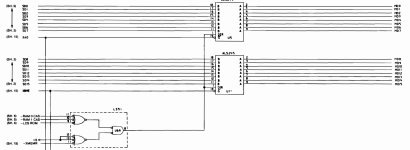
You can see the MDx lines on the right side, which go directly to the DRAM data lines as well as the ROM data lines. These buffers are enabled by a combination of XA0/XBHE, and those signals are derived from the processor signals indicating if an memory access is going to high or low bytes. The direction flag picks if the data is flowing from or to memory. If you look at the DIR line it is driven by the output of a 74LS51, which is a double 3in AND gate to a 2in NOR gate. That gate combo is connected such that if either ROM0CAS, ROM1CAS, or LCSROM is low AND XMEMR is low, to set DIR=1, which enables the buffers to drive the left side databus from the DRAM or ROM during a read op.

RAM1CAS indicates the upper 256K DRAM access, and RAM0CAS indicates the lower 256K DRAM access. (and LCSROM must be for ROM access). If we look at the source of those signals:

Screenshot 2023-03-20 at 1.25.42 PM.jpg

You can see RAM0CAS and RAM1CAS come out of a transparent latch (ALS573). That latch is driven from U72, a 28S42 512 byte PROM. That PROM acts like a logic decoder, taking the A17-A23 address bit and creates the correct RAS and CAS signals for the correct bank. You can see the RAM jumper that also feeds into that PROM which allows you to disable the upper 256K of onboard memory. We need to make both RAM0CAS and RAM1CAS inactive. RAM1CAS is taken care of with the jumper, so we just need to fix RAM0CAS.

There are a couple of options:
(1) We could cut the trace on the PCB going from U72 to U64(called RCAS0), and add a pullup at U64 pin 9 for that RAM0CAS signal. To undo the mod you would have to add a wire to repair the cut trace.

(2) We could desolder U64, and bend pin 9 up and connect it to +5V, however that would still leave the RCAS0 to U63 connection. That connection goes to that 4in NAND gate which creates F16/FSYS16. I need to look and see if that would cause a problem or not. If it does, we could just do option 1.

The parity checking circuity is selected with the RAMSEL signal , so that gets fixed in the above option to parity checking won't be a problem.
Either way, it seems pretty straightforward to make a small modification such that all of the onboard DRAM is disabled. Building an ISA card to provide SRAM for all of the system memory should be a pretty straightforward task. I have not done an ISA board in 20 years, but certainly doable.

Thoughts?

Jeff Sponaugle
 
You can see RAM0CAS and RAM1CAS come out of a transparent latch (ALS573). That latch is driven from U72, a 28S42 512 byte PROM. That PROM acts like a logic decoder, taking the A17-A23 address bit and creates the correct RAS and CAS signals for the correct bank. You can see the RAM jumper that also feeds into that PROM which allows you to disable the upper 256K of onboard memory. We need to make both RAM0CAS and RAM1CAS inactive. RAM1CAS is taken care of with the jumper, so we just need to fix RAM0CAS.
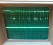
For verification, I scoped on pin9(RCAS0, upper curve) and pin7(RCAS1, lower curve) of U64 and amazingly got totally different curves, independently of jumper setting of j18. I would expect mostly identical curves here, at least when the upper 256K are enabled by j18. Swapping probes and channels made no difference. During boot, memory counts up to 384K, which is probably due to the failing stacked RAM module I'm aware of. However, by disabling the upper 256K with j18, pin6 of U64 goes low. Is the schematic misleading concerning pin-numbering here?

RCAS0RCAS1.jpg


(2) We could desolder U64, and bend pin 9 up and connect it to +5V, however that would still leave the RCAS0 to U63 connection. That connection goes to that 4in NAND gate which creates F16/FSYS16. I need to look and see if that would cause a problem or not. If it does, we could just do option 1.
If possible, I would go for this, in my opinion less inversive option. Socketing this ic makes it easily changeable in case it dies along the way (if still available though).


Building an ISA card to provide SRAM for all of the system memory should be a pretty straightforward task. I have not done an ISA board in 20 years, but certainly doable.
Never have done any... My last serious contact with the hardware side of computing was in university back in the 90th. Happy to learn something here.


If you were looking to replace DRAM with DRAM, yes you could make s small PCB that plugs directly into a DRAM socket and has a DRAM on it. There are some difficulties in that because there are no recently produced 5V DRAMs, and if you had some old ones they would probably be a lot larger in total space so you would have a lot of waste. You would also have to do some work to make sure the refresh works correctly (in particular that you get enough row reads in the allotted time).
Using SRAM (which is what Mans did) has the advantage of not needing refresh and being very compact.
Yes, voltage droped significantly with newer DRAM, forgot about that. Already thought there must be good reason that nobody has build this kind of replacement. Thanks for clarification.
 
For verification, I scoped on pin9(RCAS0, upper curve) and pin7(RCAS1, lower curve) of U64 and amazingly got totally different curves, independently of jumper setting of j18. I would expect mostly identical curves here, at least when the upper 256K are enabled by j18. Swapping probes and channels made no difference. During boot, memory counts up to 384K, which is probably due to the failing stacked RAM module I'm aware of. However, by disabling the upper 256K with j18, pin6 of U64 goes low. Is the schematic misleading concerning pin-numbering here?

View attachment 1254518

Ah interesting. I'll take a look on my board and see what it looks like. It is certainly possible the schematic is not perfect. As I understand it the XT schematic has a few mistakes in it.
You should see both RAS lines during refresh doing the same thing, but otherwise you would not see a lot on the second RAS line unless something is accessing that upper 256K region of memory. I"ll do some capture with my scope.

If possible, I would go for this, in my opinion less inversive option. Socketing this ic makes it easily changeable in case it dies along the way (if still available though).

Yea, that makes sense. I'll double check the trace layout and make sure this is how the actual board is built.
Never have done any... My last serious contact with the hardware side of computing was in university back in the 90th. Happy to learn something here.

This will be a pretty easy PCB to build. I put together a completed schematic in a few hours. I'm using DipTrace which is a particularly easy schematic and PCB tool. For the SRAM I'm using AS6C4008s, which are DIP package 512kx8 SRAMs that can be purchased new (and I have a ton of them already). I'll start off with 2MBs, but it will be easy to add some more banks.
For the interface logic, I am going to use an ATF1504 CPLD in a PLCC44 package. It is overkill for this, but since I'm not 100% sure on all of the signaling it will be a great way to be able to test the logic. I have used the ATF1504s and 1508s on a ton of different projects, and they are on of the only CPLDs available new today that are 5V and fast (7.5ns). I'll order the PCBs from JLCPCB, so it should only take 5-10 days to get the PCBs back and start testing.

Yes, voltage droped significantly with newer DRAM, forgot about that. Already thought there must be good reason that nobody has build this kind of replacement. Thanks for clarification.

Yea, in general 5V parts are getting so much harder to find in new form. 3.3V parts are still available, but even that is starting the decline. Given how inexpensive SRAM is (these 512k are around $6), it makes it easy to use.
 
Back
Top