• Please review our updated Terms and Rules here

A New S-100 Bus Master/Slave 80386 CPU Board

monahan_z

Experienced Member
Joined
Oct 19, 2008
Messages
263
Location
San Ramon, CA
For people interested in building/repairing S-100 systems, Andrew Lynch at N8VEM and I at S100Computers.com have just completed a prototype of a new 80386 Master/Slave CPU board. This exciting board is capable of reaching up to12MHz in an S-100 system with an active terminated bus.

This is an ongoing project. It utilizes the 16 bit mode of the 80386 to address the 16MG of RAM the S-100 bus is capable of addressing. A second daughter board system with an overhead ribbon cable connector is planned to for daughter board(s) to enlarge the RAM space up to the 4GB the CPU is capable of addressing (using high density static and DRAM chips).

If you would like to read about this board please look here:-
http://s100computers.com/My System Pages/80386 Board/80386 CPU Board.htm

There is a growing list of people getting interested in these S-100 systems. We get these bare boards produced in batches (typically $20-40, depending on demand). We have done over 20 different types of S-100 boards so far! It is too early to accept “orders” for this board, but if you would like to be kept in the loop as this board evolves keep an eye on the above page.
 
Is the idea to be able to run this in a vintage s-100 system or to build your own new s-100 system with your other boards? Great work on all the boards, I can't believe how many you all were able to whip out.

Separate project but perhaps not that feasible, could there be a generic s-100 diagnostic board? Something to help diagnose issues with an existing s-100 setup?
 
Hi barythrin, there is not a major long term goal in sight. The 80386 will probably be the end of the line for Intel chips for now. May do a 68020 (or heigher), but the next CPUs I am thinking about are the more recent/current ones, ARM's etc. However between getting a GB capacity DRAM board and a SVGA graphics board going I think we will be fully occupied for the next few months.

A diagnostic board is a possibility. I'm thinking some kind of PIC or Propeller driven system. However to catch many bus problems its fairly difficult to do. The SMB and a few tricks in small software routines in most cases quickly identifies problems. But I will think about it.

Along those lines I would be interested in hearing what people would like to see in such a board.
 
But do you (or anybody out there), have a schematic for such a DRAM board. What controller, what do you do when the 80386 is no longer the master CPU on the bus, how do you handle a vastly different clock speed for DRAM access and S-100 bus (static) access. I thinking a VT82225N. I would like to avoid re-inventing the wheel. Just bring PC like capability to the S-100 bus. Any help will be gratefully accepted
John
 
I recently found a couple of versions of the MSDOS Boot Prom used with the Compupro Disk-1 (will probably work on the Compupro Disk-1A with 8" floppies also) to boot up the special versions of MSDOS on Compupro S-100 Systems. I thought I lost or got rid of them when I sold the MSDOS on 8" floppy years ago. Now I'm thinking that since I kept copies of the Proms, I may have kept backup copies of the MSDOS for the customers that bought the MSDOS from me.
 
You could do SDR DRAM or possibly single rate DDR with a PLD as long as it's less than 100 MHz. I've done the former. The later generally requires a licensed core but there are exceptions like Milkymist. With both, you are looking at single chip capacities up to 64 MB (16 or 32 bit) and DIMM capacities up to 512 MB (64 or 128 bit). But you are solidly in SMT territory with matched traces and termination resistance - even for SDR. Anything higher capacity than that and you are in to DDR2/3 with DLLs that have minimum lock frequencies well above 100 MHz or fully static LPDDR that is generally BGA/POP only. Both require multi-layer controlled impedance boards at prohibitive costs in small quantities.

You said "GB capacity" with a capitol B. If you mean gigabyte, it's just not going to be possible unless you use something like a pre-fabbed FPGA module. I suggest going with a module like the Lava 10 you've used before. I've also layed out a similar board with a MachXO2 that is 5V tolerant, has configurable I/O, and can be reprogrammed via a serial port. There might be enough interest to take that further.
 
Very interesting eeguru! You have quite a few things there I did not know.
First I realize for any kind of decent RAM capacity we will have to go to SMT chips. Currently I'm thinking doing a simple all static RAM daughter board with something like ISSI 512X16 CMOS RAMS (IS62WV51216ALL) or the Cypress equivalent (CY62167DV30). This would allow us to work out bugs in the daughter board connection/bus etc. before going to a DRAM board. Should be able to get to at least 8Mg/board with that. (They are large chips!)
After that looks like we have to go to some kind of DRAM. I am out of my depth here. I had hoped I could use cheap/common SIMMs with Gigabyte capacity. If I understand you correctly, it seems you need clock frequencies in the 100 MHz range for these chips. Is that the bus speed?
Could I ask you the core question I am trying to determine: What is the easiest way to add as much DRAM to an S-100 size daughter board with connections directly to the 80386 CPU pins (via drivers). Assume the CPU does not even know it is also connected to the S-100 bus for I/O etc.
Is there a refresh controller you would recommend? Is there an example schematic? This would not have to be the fastest RAM possible. I’m more interested in capacity over speed.
Are Pseudo-static RAM’s a possibility? Can one get to Gigabyte capacity boards with them without costing a small fortune.

There is a LOT of sd ram on the market. wouldn't it be easier to use existing pc133 ram? I know 1gb modules are pretty common. I know 2gb modules exist but were pretty special. :p
 
I had hoped I could use cheap/common SIMMs with Gigabyte capacity. If I understand you correctly, it seems you need clock frequencies in the 100 MHz range for these chips. Is that the bus speed?

The >100 MHz is the DQ clock for DDR2/3 ram parts. DDR2/3 doesn't support fully static operation unlike LPDDR, some single rate DDR parts and pretty much everything before. You have to maintain a minimum clock otherwise the DLL will lose lock on the incoming reference and stop working.

Why you are interested in gigabytes for an S-100 system? That seems a little wonkey to me. 2.4 Linux kernels will run quite happily in 16MB or even less. For GUI applications, 64MB seems overkill to me. I don't even want to think about how long a 1GB memory check would take on a 386/16 either.


What is the easiest way to add as much DRAM to an S-100 size daughter board with connections directly to the 80386 CPU pins (via drivers). Assume the CPU does not even know it is also connected to the S-100 bus for I/O etc.
Is there a refresh controller you would recommend? Is there an example schematic? This would not have to be the fastest RAM possible. I’m more interested in capacity over speed.

DDR2/3 is completely out, even with DIMMs, due to minimum lock range of DLLs, low noise immunity, high speed requiring impedance control and lack of suitable controllers in leaded packages.

That leaves SDR SDRAM as the next step. A PC133 SO-DIMM would be possible if you are looking for just a whole lot of capacity (up to 512MB). However there's 105 nets there alone + bus interfacing to the backend. That's going to be pushing the pin count for most leaded parts. If you cut the data and DQ strobes in half and only use 32-bits, it might be doable on Spartan 3/6 or MachXO2. That would leave 25+ signals for bus interfacing. Which would still mean having to implement paging/windowing in the controller.

If you want something that is full 32-bit to both RAM and bus, it's a minimum 117 signals just for a single 32MByte chip. Again going to be very difficult to accommodate that in a leaded part.

I suggest starting with a single chip 16-bit data design and moving up. Or possibly a legacy design using 30 or 72-pin SIMMs. I'm sure there are a lot of legacy DRAM controllers that would be suitable. However once you get into the fast page mode era, most if not all went to leaded SMT. So finding them will mean locating back stock through brokers rather than working pulls. Did you guys ever get the 68040/68360 design working?

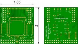
You can start with a new design using a FPGA and even leverage the FPGA to eventually do more. Here is the design for the module I previously mentioned. You could do it with just about any FPGA, I just prefer Lattice. I'm not sure how much guidance I can give you beyond that as I get trickles of time here and there to work on these things and it's always possible I could be out of touch for weeks at a time due to work. But can keep answering questions.

mezz.jpg

Can one get to Gigabyte capacity boards with them without costing a small fortune.

Not really.
 
Yes, but how do you refresh the DRAM. What I am looking for is a reliable circuit to refresh any of these common SIMMS. An Intel motherboard North/Southbridge type of thing is too difficult.
 
It's just not that simple. Most parts past simple discrete DIP chips have internal auto-refresh. Parts now are banked and paged internally and must be command controlled with a fairly complex finite state machine. Care must also be given to minimum transition times between states. Take a look at the state diagram on page 15 for this SDR SDRAM chip and you'll get a feel for the complexity involved.

You are not going to able to just plop down some DIMM sockets, wire up a few combinatorial gates, and a timer to periodically stroke CAS.

You will need a legitimate fully buffered DRAM controller. You might have luck finding some overstock ASIC to do older tech (EDO, Fast Page Mode, etc). But if you want to use current cheap SDR or DDR1 SDRAM devices (discrete or DIMM), you're best bet is to turn a small FPGA or a large CPLD into one. SDR and DDR1 SDRAM is very common in PLD projects so there are numerous free IP cores for it.

SIMMs still have the same state machine complexity (more if EDO or FPM) and offer less density than the controller/single chip board above.
 
Last edited:
Did you guys ever get the 68040/68360 design working?

Hi

The MC68040 SBC project continues but it is a completely separate project from the S-100 80386 CPU board. Both projects share the need for a large system RAM and the MC68040 SBC is planned to use an MC68360 QUICC to control a couple of SIMMs (72 pin *not* PC-133) for 256MB. At the moment it is an intermediate prototype "MC68360-P1" for proof-of-concept of the all important MC68360 chip with a bare-bones flash ROM and two small SRAMs. We've made some prototype PCBs but those are not booting yet but hopefully will be soon. The MC68360 is a complicated chip with a lot of variants so it is not terribly surprising it is difficult to get it going.

It does raise some interesting possibilities though if a 80386 could interface to an MC68360 as a large DRAM controller. I have no idea if that is possible or not but it is moot until we get the MC68360-P1 prototypes working. Getting more MC68360-P1 prototype boards would be fairly simple if anyone wants to take a whack at it and I believe Dave would appreciate another set of eyes on it. The MC68360 is a sophisticated processor by itself and can be interfaced to MC68030, MC68040, other MC68360s and probably other CPUs. If it does work it could be a common solution for the MC68040 SBC and the S-100 80386 CPU board.

Assuming a marriage between an 80386 and MC68360 is even possible it would have a tremendous advantage in that 100% of the parts are 5V PTH compatible including the SIMM sockets and the MC68360 PGA. I think it would be fairly easy to fit an MC68360 plus glue logic and 2-4 SIMMs on an S-100 mezzanine board. Also the MC68360 chips seem readily available in QFP and PGA formats.

Thanks and have a nice day!

Andrew Lynch
 
Last edited:
Thanks for the status update Andrew. I remembered you guys hitting this need before.

Couple additional notes worth considering: Both the Motorola/Freescale reference design for 68040/68360 and the National app note for interfacing a DP842xA to a 80386 (another completely PTH solution) both call for a couple PALs as glue. So it's unlikely you will be able to escape programmable logic to some degree to add a non-trivial amount of SDRAM. Second I've updated the design above to enlarge the board a bit (1/2" in one dir) to include an on-board programmer w/ mini-USB port in place of the MCU. The entire BoM cost of that board (minus headers) is still less than the cost of one MC68360 PGA and that gap will continue moving in the wrong direction. It's entirely reasonable with enough interest via a kickstart to have boards made for not much more. It could be a way to add 32MB RAM/32MB ROM plus other to be developed uses (eg VGA controller) to a variety of projects. I plan on ordering some prototypes this weekend in any case.
 
For the 80386 CPU, I think the DP8422A is our best bet with the highest chance of success. It is designed to work with the 80386 and is still available.

It won't provide enormous RAM sizes but should be sufficient for Linux and/or BSD.

Thanks!

Andrew Lynch
 
Thanks so much eeguru for your insight. Unfortunately I naively thought you could "plop down some DIMM sockets, wire up a few combinatorial gates, and a timer to periodically stroke CAS". Just looking at page 15 for the SDR SDRAM is just downright scary! That, and the schematic mentioned, illustrates to me there is no way I alone could implement something in that range with my current state of knowledge.

I’m not clear on how a FPGA/Spartan approach works BTW. Is it the Spartan “does its own thing” refreshing DRAM etc. and is setup to have an internal program that takes 32 data lines (emulating RAM to the 80386) and stores/sends them to/from its own RAM. If so, can it really keep up to the data rate of an 80386 without many wait states?

I now thinking perhaps we should settle for a simple static RAM board. The best I’m seeing so far are things like the Cypress 1MX16 (CY62167DV30)’s 48 pin TSOP’s. These are ~0.8” X 0.5”. So Andrew could probably get at least 24 of them on an S-100 “daughter board”. That would give us 48MG. Problem is it would be one hell of an expensive board. But backing off in capacity however one could probably get to 16MB at a reasonable price.

Any suggestion where the “sweet spot” is capacity/price wise for Static RAM chips.

Andrew for your DP8422A, we may as well go Static RAM. It seems to me to be a large chip for little RAM capacity. Am I missing something?.

Eeguru, what do you think of pseudo-static DRAMS. Would they be easier to implement. What capacity do you think one could get on an S-100 board of the type we discussed? Is there any possibility of a “plop down some DIMM sockets, wire up a few combinatorial gates, and a timer to periodically stroke CAS” tor that situation?

John
 
There are numerous free cores written that implement the SDR state transition logic in Verlog or VHDL. You can use pretty much any PL device from Altera, Lattice, Xilinx, and others. There are even papers written by engineers at all of those companies for older devices for older RAM technologies. They might be insightful reads - especially on how the state transitions evolved through EDO, FPM and finally to SDR SDRAM.

Essentially the board described above and others like it will turn a SDR SDRAM part into what will look like a fully asynchronous 32MB parallel SRAM to the host processor. The timing of DRAM requests are not always deterministic depending on whether the request can be serviced by a prior burst, if it comes from the same row or column on the active bank, or active refresh cycles. So one of the lines coming back from the FPGA would be an open drain ready signal. When the FPGA is selected - either with an external CS or one generated from an internal address decode - it will drive ready down until the buffered DRAM state machine returns the data asked for. There are 48 5V tolerant expansion I/Os on the above module. For example you could assigned those to A[1..24], BHE, BLE, D[0..16], /WE, /OE, /RAM_CS, /ROM_CS, READY, and /RESET with an image file intended for 16 bit system. Or some other combination for different systems and applications (such as a Lava 10 replacement).

Also in the above design is up-to a 32MB QSPI flash that it will flatten out into a linear address space so that it looks like a static parallel device. You could also do interesting things like DMA and ROM shadowing if you so desired.

The whole thing is a condensed down version of a 16-bit 32MB ISA EMS/XMS board I'm currently working on.
 
Last edited:
eeguru, I just came across these ISSI pseudo-static RAMS (IS66WVE4M16BLL) see:-
http://www.issi.com/pdf/66WVE4M16BLL.pdf
They are 4MegX16 and are available in single unit quantities (http://www.onlinecomponents.com/issi_is66wve4m16bll-70bli.html?p=43095856) for $3-4 each.
They are available in 48-pin TSOP-I package as well. Could easily fit fit 16 or 20 Meg on a board with costing an arm and a leg.
Am I missing something because that arrangement would look like a "plop down a RAM and a few connecting chips".
 
Back
Top