Mike_Z
Veteran Member
My CP/M 2.2 machine is a 64K 8080 machine. I have a parallel peripheral interface PPI that uses a 8255. I have found that the outputs are not strong enough to drive too much and generally cause some trouble. A year or so ago I added some buffers 74LS244's to the outputs, which helped tremendously, but I wired them in for output only. I have decided to try and improve this by attempting to program the I/O buffers whenever the PPI is programmed. I decided to only use Mode 0 or the PPI, yet have the ability to divide port C into two 4 bit ports and to have any combination of input and/or output of 4 ports. I had thought that if I could set 4 flip flops according to the Control Register programming I could direct the buffers for proper I/O. So, basically I clock 4 positive edge FF from the control register chip select and the write signal. The flip flops have their data line connected to D0, D1, D3 and D4. These data lines, when WR go low, will have Mode 0 I/O information.
I wired up a circuit and it doesn't work as I had projected. Seems that the FF's are trigger a little early.
I used this test program to see this.
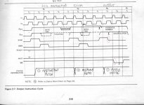
Single stepping through this program, shows it should work, but turns out the timing is a problem. So I pulled out my 8080 handbook and began reviewing machine cycles again. I don't completely understand the OUT (or any other instruction). According to the 8080 Handbook on page 2-9, figure 2-7 shows the Output instruction cycle. There are 3 machine cycles, which have 4,3 and 3 clock cycles in them. Additional OUT instruction cycle information is shown on page 2-18.
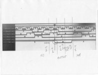
Using the logic analyzer, I monitored the #4 Data Line (this signal controls the I/O of Port A during WR low), Write line and Phase 2 TTL lines. I thought that I could compare these traces with what I saw in the Handbook. But.... as usual something is different.
I copied this right from the handbook, regarding the OUT instruction Machine cycle 3, 'the rising edge of Phase 2 within state T2 clears status info from the CPU's lines and loads in the data which is to be output to external devices. This takes place within the Data Output Delay TDD, following the Phase 2 leading edge (220nSec).' This tells me that the data I want to output to the control register of the PPI should be on the data bus at the end of clock cycle T2. Then when WR goes low in T3, my FF's should capture the I/O data. But this does work this way. I tried data of 200 (octal) which corresponds to Port A output. The D4 of 200 is a zero, yet my FF is set, indicating that D4 was high when the positive edge clock pulse occurred. This is confirmed by the logic analyzer trace.
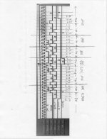
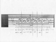
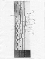
Here is a picture of the Logic analyzer trace.
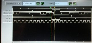
The CLK trace is the positive edge trigger for my flip flops, Data is the data bus line 4, Q is the output of the port A flip flop, ~WR is the WRITE (knotted) signal and Ph2 is the phase 2 clock pulses. You can see the my flip flops are trigger when the ~WR goes low (this is actually the PPI chip select AND ~WR). You can also see that D4 is high during the trigger. I figured that D4 should have been a zero since the end of M3 T2. Another unusual indication in this graph is that ~WR stays low for two clock cycles, not one. My machine does not use any wait states for anything. This is why I'm thinking that the ~WR signal is one clock cycle early, If ~WR were to wait one more clock cycle, D4 would be correct. I also tried this with the D4 being high, if ~WR was delayed one clock cycle here also, D4 would be correct.
Anyway, I'm studying the instruction cycles in an attempt to better understand what I'm seeing on the logic analyzer. D4 shows it is zero four different times during the OUT instruction. Obviously, the data bus must be used for items like incrementing the Program counter etal. Seems the more I learn, the less I know. Mike
I wired up a circuit and it doesn't work as I had projected. Seems that the FF's are trigger a little early.
I used this test program to see this.
Code:
MVIA 200	;Code for all PPI ports to output
OUT  157	;157 is the CTRL REG of PPI
HLTUsing the logic analyzer, I monitored the #4 Data Line (this signal controls the I/O of Port A during WR low), Write line and Phase 2 TTL lines. I thought that I could compare these traces with what I saw in the Handbook. But.... as usual something is different.
I copied this right from the handbook, regarding the OUT instruction Machine cycle 3, 'the rising edge of Phase 2 within state T2 clears status info from the CPU's lines and loads in the data which is to be output to external devices. This takes place within the Data Output Delay TDD, following the Phase 2 leading edge (220nSec).' This tells me that the data I want to output to the control register of the PPI should be on the data bus at the end of clock cycle T2. Then when WR goes low in T3, my FF's should capture the I/O data. But this does work this way. I tried data of 200 (octal) which corresponds to Port A output. The D4 of 200 is a zero, yet my FF is set, indicating that D4 was high when the positive edge clock pulse occurred. This is confirmed by the logic analyzer trace.
Here is a picture of the Logic analyzer trace.

The CLK trace is the positive edge trigger for my flip flops, Data is the data bus line 4, Q is the output of the port A flip flop, ~WR is the WRITE (knotted) signal and Ph2 is the phase 2 clock pulses. You can see the my flip flops are trigger when the ~WR goes low (this is actually the PPI chip select AND ~WR). You can also see that D4 is high during the trigger. I figured that D4 should have been a zero since the end of M3 T2. Another unusual indication in this graph is that ~WR stays low for two clock cycles, not one. My machine does not use any wait states for anything. This is why I'm thinking that the ~WR signal is one clock cycle early, If ~WR were to wait one more clock cycle, D4 would be correct. I also tried this with the D4 being high, if ~WR was delayed one clock cycle here also, D4 would be correct.
Anyway, I'm studying the instruction cycles in an attempt to better understand what I'm seeing on the logic analyzer. D4 shows it is zero four different times during the OUT instruction. Obviously, the data bus must be used for items like incrementing the Program counter etal. Seems the more I learn, the less I know. Mike

