• Please review our updated Terms and Rules here

Ever run into this? ROM data lines mismatched vs CPU

westveld

Experienced Member
Joined
Dec 31, 2009
Messages
172
Location
Reed City, MI
The SYSCOM II Apple II+ clone I've been working on is weird.

The ROMs data lines are wired like this:

Code:
CPU D0 -- ROM D7
CPU D1 -- ROM D1
CPU D2 -- ROM D2
CPU D3 -- ROM D4
CPU D4 -- ROM D3
CPU D5 -- ROM D5
CPU D6 -- ROM D6
CPU D7 -- ROM D0

Maybe they did this on purpose to avoid copyright somehow?
In the end the ROMs are almost identical to Apple's.

I dumped the ROMs and was confused - I expected almost identical to Apple II+ ROMs, but they are completely different.

And they don't match what the computer sees in monitor either.

I first assumed I goofed up the wiring on the ROM dumper, but no - dumped some other ROMs and they matched the expected images exactly.

Then assumed it was address lines not as expected, but nope - cheap logic analyzer on the data lines showed the expected ROM did send 1 thing out and the CPU got something different.

Ahah, take another look at comparing the binary of the monitor dump and the ROM dump and figure out the line flipping.

Sheesh
 
If you think about it, the address and data line labels on a PROM are largely arbitrary. We assume that D0 is D0 because that datasheet says it is.
Not the case, however, with DRAM, where multiplexed addressing matters to some extent.
 
The original SpeedDOS in the Commodore 1541 drive did the same. There was also the antivirus program ThunderByte that had its own card with an EPROM on it and means to disable writing to a floppy disk and/or IDE HDD. You may already have guessed, (some of) the data lines have been mixed up as well. I still use some of these cards for my 286+ machines to install the Universal BIOS so I could handle bigger HDDs. But I had to write a little program first that mixed up the bits before I could burn the EPROM.
 
If you think about it, the address and data line labels on a PROM are largely arbitrary. We assume that D0 is D0 because that datasheet says it is.
Not the case, however, with DRAM, where multiplexed addressing matters to some extent.

Hm, would the same be true for address lines, at least on reading ROM/EPROM ?

I wounder what the designer would think about this thread 40-ish years later. Fooled another newb for a while, haha!
 
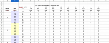
Sure, I ran into this when I decoded the Radio Shack KSG Tech Lowercase EPROM board. The address Lines were going to different
Address Pins on the EPROM and I used an excel spreadsheet to figure out the addressing. It was interesting that they spent that much
effort to use the same Characters in the EPROM.

Larry

Model1CharGen.png
 
It may not have been effort to obfuscate the ROM, it may have been physical layout on the board. I often use the same trick with SRAM chips where mixed address and data lines don't really matter. Wire the lines to the bus in the most convenient manner, not worrying about order, fix the ROM image once you know the layout.
 
SRAM, OK, I do the same trick with my designs. But ROM? Assuming that the lines are mixed differently for every design means a different program to fix the image. If others start using your design it means you have to provide that program. But if users have to program a new EPROM because of (own) enhancements and bug fixing and therefore have to use this program every time.... I personally don't consider this user friendly. (no offense meant)
 
I'm with Jim on this one--avoid having to do fancy trace routing can mean a more compact PCB and that means money. I can see where having the PROM bits in reverse order from the datasheet may make sense.

A similar situation obtains when, say, a LFSR is used instead of a counter--all the bits get covered, just not in consecutive order. May simplify the design considerably.
 
Back
Top