eeguru
Veteran Member
This is a reposting of a post I made over on Mike's PCjr Forums. Thought it might have more interest here since there's more visitor traffic.
-Alan.
-------------------------------------------
Speaking of theoretical, after thinking of this thread a while, I wondered if it would be possible to design a board that literally fit into the footprint of an 8088? For systems (not just the PCjr) that were ether space constrained around the processor socket or had limited or no ISA expansion slots for RAM cards (eg. most early Tandy 1000 systems and IBM 5150s). So I tried it. I can say it's theoretically possible, though to actually build it would require about $500 just for PCBs (qty 1 to 50+ doesn't matter due to NRE) since it's 4 layer, has an abnormally high via density, 6/6 tech, and small to the point you lose a lot of efficiency on panels.
It's basically the exact footprint of a 40-pin DIP socket (2.2" x .7") plus a couple millimeters overhang on the front edge for three 2mm jumpers to allow changing of the RAM map after assembly/programming. At build time, the code can be configured for a minimum mode system (eg. PCJr, Tandy's, etc) or a maximum mode system (most PC/XT clones). And the jumpers provide 8 possible memory fill maps each with 32k resolution. Basically they feed into a lookup table along with A15-A19 with the RAM chip selects as outputs. They then get gated with the control strobes and routed to pads. The 8 memory maps could be customized on a order/build basis by changing the lookup tables before programming the PLD. If not, I can think of a few generic ones that would be useful.
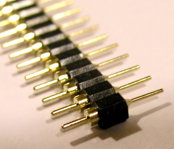
It has 2x 512KB SRAMs on the top side of the board that sit in the reliefs provided by this wire wrap socket. On the bottom side, there are a couple latches, a buffer, and a 22V10 PLD. Everything is TSOP so the wire wrap pins could be cut down a bit so it adds less than a half inch to the processor height. Though with all the chips stacked, heat might be an issue - even though everything is HCMOS.
I put together a rough BOM to try and price things out if there were enough interest in a production run. It's all SMD/SMT so it would not be user assembly friendly Though it would be an open source hardware project - so you could free-build. The total parts cost including PCBs at a 25 unit run with some NRE factored in (Kapton stencils, solder paste, TSOP programming adapter, etc), is ~$45.00. I don't have a lot of time to program PLDs, assemble, clean and package boards, so I would tack on $25 (not including shipping) to help mitigate some of that; which is ~2/3 cheaper than most web assembly quotes I found and those only cover assembly. Not to mention fronting $1200. So if there is interest... and I can't imagine there would be much.. post here and maybe we can get enough people together to give me a warm and fuzzy about selling at least 20 of the boards. Otherwise, PM me for the Eagle files and PLD code if you are interested. It was more of a mind exercise than a serious idea anyway.
PCB Layout
Schematic
Bill of Materials
-Alan
-Alan.
-------------------------------------------
Speaking of theoretical, after thinking of this thread a while, I wondered if it would be possible to design a board that literally fit into the footprint of an 8088? For systems (not just the PCjr) that were ether space constrained around the processor socket or had limited or no ISA expansion slots for RAM cards (eg. most early Tandy 1000 systems and IBM 5150s). So I tried it. I can say it's theoretically possible, though to actually build it would require about $500 just for PCBs (qty 1 to 50+ doesn't matter due to NRE) since it's 4 layer, has an abnormally high via density, 6/6 tech, and small to the point you lose a lot of efficiency on panels.
It's basically the exact footprint of a 40-pin DIP socket (2.2" x .7") plus a couple millimeters overhang on the front edge for three 2mm jumpers to allow changing of the RAM map after assembly/programming. At build time, the code can be configured for a minimum mode system (eg. PCJr, Tandy's, etc) or a maximum mode system (most PC/XT clones). And the jumpers provide 8 possible memory fill maps each with 32k resolution. Basically they feed into a lookup table along with A15-A19 with the RAM chip selects as outputs. They then get gated with the control strobes and routed to pads. The 8 memory maps could be customized on a order/build basis by changing the lookup tables before programming the PLD. If not, I can think of a few generic ones that would be useful.
It has 2x 512KB SRAMs on the top side of the board that sit in the reliefs provided by this wire wrap socket. On the bottom side, there are a couple latches, a buffer, and a 22V10 PLD. Everything is TSOP so the wire wrap pins could be cut down a bit so it adds less than a half inch to the processor height. Though with all the chips stacked, heat might be an issue - even though everything is HCMOS.
I put together a rough BOM to try and price things out if there were enough interest in a production run. It's all SMD/SMT so it would not be user assembly friendly Though it would be an open source hardware project - so you could free-build. The total parts cost including PCBs at a 25 unit run with some NRE factored in (Kapton stencils, solder paste, TSOP programming adapter, etc), is ~$45.00. I don't have a lot of time to program PLDs, assemble, clean and package boards, so I would tack on $25 (not including shipping) to help mitigate some of that; which is ~2/3 cheaper than most web assembly quotes I found and those only cover assembly. Not to mention fronting $1200. So if there is interest... and I can't imagine there would be much.. post here and maybe we can get enough people together to give me a warm and fuzzy about selling at least 20 of the boards. Otherwise, PM me for the Eagle files and PLD code if you are interested. It was more of a mind exercise than a serious idea anyway.
PCB Layout
Schematic
Bill of Materials
-Alan

")