Theodric
Member
Long-time lurker, first-time poster. This is ultimately a cry for help, because it’s not working, but I’m an excessively wordy person so there’s a long preamble before I get to it.
Picture gallery: https://imgur.com/gallery/tZA85
—BACKGROUND—
A couple months ago, I acquired a Heathkit H11A from a seller in the USA. The seller reported having powered it up, but did no other testing, since he’s not a techie guy. It had evidently sat in a storage locker for quite some time, and found its way to eBay when he was tasked with clearing out the estate of a former CDC engineer by the widow. He shared the anecdote that one of the H89s occupying the same storage locker found its way into Stranger Things, and that Netflix was not bothered about paying an additional $300 for next-day shipping on a system they’d bought for $300. That’s about as nearby to fame as I’m ever likely to get, so I’ll take it.
It arrived in fairly good shape, apart from the fact that all but one of the expansion cards had shaken loose during shipping. (I don’t see any obvious damage to any of the cards.) One of the brass screw insert lugs on the side panels had cracked the boss it was installed in, but I was able to reassemble and patch the boss with two-component resin: it’s almost, but not entirely, invisible. There was a small amount of surface rust on the steel parts, and a couple tiny patches of aluminum corrosion elsewhere, but the casing otherwise looked good.
Based on this post, I surmise that the Heathkit backplane is Q16 configuration, which will need to be modified to support 18- and 22-bit cards: https://groups.google.com/forum/#!topic/alt.sys.pdp11/YwsiIH3rWe8
The system contains five cards:
-DEC M7270 LSI-11/2 CPU with the optional 3015D EIS/FIS IC socketed
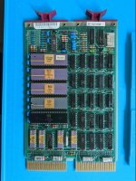
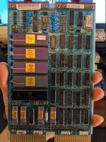
-An anonymous 32KW memory card, populated with 32 ITT 4116 SRAM ICs. It looks like a hand-built commercial product (“ASSEMBLED IN MEXICO”), with a high-quality etch and mask job, but handwritten S/N and P/N and what looks like a hand-drawn layout with manual scoring between some close-together traces. No manufacturer listed. I wasn’t able to locate any information on the card by searching the P/N, but maybe someone will recognize the card.
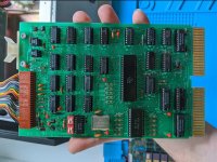
-A Heathkit H-11-5 serial card, with attendant breakout cable and DB25 adapter
-An Andromeda Systems FDC-11B and its 50-pin cable. I surmise that this is a Floppy Disk Controller, but found no useful information online.
-An Andromeda Systems LPI-11 and its Berg to flat cable to Berg to Centronics-breakout-PCB thingy. I surmise that this is a Line Printer Interface, but again, found nothing online.
—RESTORATION WORK—
I focused first on ensuring that the PSU wouldn’t kill anything (assuming the seller’s smoke test hadn’t done so already) by replacing all of the PSU’s electrolytic capacitors, both cans and tantalums, as well as one crusty 7805 and one 74LS00. (The tants might have been fine, but I’ve seen too many “Roman candle” failures in Commodore PETs to want to toy with that. Apart from the 74LS00 that I found was causing RUN/HALT to stick high, all of the removed components including the elderly 7805 tested out fine.) After all that was done, I dialled the PSU in according to Heathkit’s specifications and ran through all of the preflight checks (apart from intentionally blowing the fuse) with success. I am therefore relatively comfortable in stating that the PSU is working according to plans. Based on http://www.classiccmp.org/cini/heath_h11.htm it seems that my H11A is one of the earlier ones with no front-panel control over the LTC/EVNT signal. The PSU will generate it unless a jumper is set appropriately to disable. That explains why my VOM measures a constant ~5V on EVNT.
—BRING-UP FAILURE—
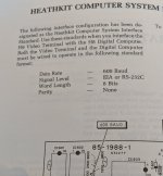
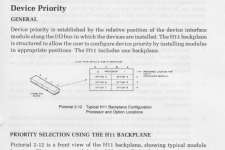
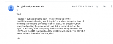
I found conflicting information online about the correct order of modules in the backplane, but the possible permutations are few: either the CPU goes on the left and the SRAM on the right (majority vote) or the opposite (minority). The Heathkit docs all assume the original quad-width PDP-11/03 CPU card, rather than the M7270, so they were of no help. The system showed marginally more signs of life in the first order, so I stuck with that.
The SRAM card has 16 DIP switches, which I surmise are bank selects, based on my reading of the DEC M8044 documentation. When I received it, the 16th switch (top 4KB?) was turned off, which I believe is explained on http://www.classiccmp.org/cini/heath_h11.htm by the following: “Since I/O devices are memory mapped, the upper 4kw of memory is disabled resulting in a net 28kw of memory.”
With CPU in top left, SRAM in top right, and serial directly under the CPU, with RUN/HALT switch in either position, the RUN light pulses twice when DC power is switched on, and once when DC power is switched off. I have yet to determine what, if anything, this signifies. No output is observed on serial.
If I toggle all the SRAM card’s DIP switches off, the RUN light stays on when DC power is switched on regardless of RUN/HALT switch position; toggling them any other way has no apparent effect, otherwise.
The M7270 CPU card has four different startup modes: one which attempts to boot from a given address and falls back to μODT on failure, one which always drops to μODT, one which attempts to boot from another address and prints that address to the screen if it fails, and an unused 4th mode for future use. I tried all of them, but none resulted in any output on serial. I also tried enabling and disabling jumper W3 (EVNT interrupt), but it changed nothing. I confirm that jumper W1 “Master Clock Enable” is wire-wrapped closed on my CPU card.
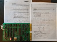
I ran through the documentation for the serial card and confirmed that it is configured according to the factory recommendations, putting the card at the correct address to function as a console @ 600,8,n,1.
I pinouted the cable supplied with the serial card and confirmed that it is wired such that it should be able to talk to my PC’s serial port with a null modem cable in between.
I removed, cleaned, and reinserted all ICs on the serial card (some were blackened with corrosion), but there was no change. Nearly all of the components on the serial card are commodity 7400-series logic, and the remaining two are widely available.
—CRY FOR HELP—
Since the M7270 has no RAM onboard, the minimum viable configuration would seem to be the CPU, RAM, and serial cards.
I bought a couple M8043 DLV11-J cards from Sellam, but do not have them yet.
Since the backplane is evidently Q16, I would need to bus BDAL16 and BDAL17 to make it Q18-compatible, a prerequisite for using later CPU cards or e.g. M8044 RAM modules (which, based on http://web.frainresearch.org:8080/projects/pdp-11/memory.php are 16-bit memory but require an 18-bit bus). I’m not sure if the M8043 requires Q18, either. Because the H11’s backplane is not identical to comparable DEC backplanes, I can’t make use of existing templates for DEC H9xxx backplane upgrades, so I’m not immediately sure what solder points I need to join up to achieve this.
The backplane does have a single additional wire connecting two pins on its third row. I have not yet tried to ascertain what this is for, since I’m only using the first two rows at this point.
Help, please? Not sure where to go from here. I am not an EE, but rather a failed Baroque cellist with an interest in vintage computers and a passing ability to read documentation and follow clear instructions, but please assume you’re talking to an idiot. I solder quite competently, and own a VOM and a cheap oscilloscope.

