• Please review our updated Terms and Rules here

ISA Extended memory board repair

rvdbijl

Experienced Member
Joined
May 8, 2017
Messages
112
Location
NH, USA
Hi All,

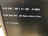
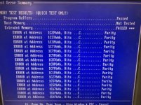
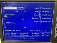
I have this 2MB 16-bit ISA board, Micron, (extended memory) that has at least one bad IC on it. When I run the Checkit memory test, the test fails in one 256K segment (the second on the board), and claims it's all parity, C.
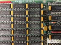
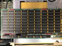
Looking at the board, it looks like the IC's are arranged in a grid of 9 x 8 (h x v). Is it safe to assume that the 9 across the top are the first 8 bits and parity for each 256k segment (8 segments = 2 MB)? If so, I'd guess that the last IC on the second row may be bad... I was going to see if I can find any of those types of ICs on eBay and try to replace that one. But I figured I'd check with the experts here to see if you concur that would be the bad one before I start pulling it off the board...

Thanks!
file1-4.jpg
file2-2.jpg
file-10.jpg
 
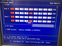
After realizing there is a RAM layout / chip finder in Checkit, it came up with this. Does that seem to make sense?
file1-5.jpg
file-11.jpg
 
I have this 2MB 16-bit ISA board, ...
16-bit. Therefore, each bank consists of 18 chips (16 data chips + 2 parity chips).
Therefore, based on the card photo, your card has 4 banks.

Each bank will be 512 KB sized (2 MB / 4).

From that, we can deduce that the chips are 256 Kbit ones (16 data chips of 256 Kbit each = 4096 Kbit = 512 KB).

After realizing there is a RAM layout / chip finder in Checkit, it came up with this. Does that seem to make sense?
It is up to the designer as to how the banks are laid out. The banks could run 0 to 3 from top to bottom, or vice-versa, or some other way. And within a bank, the data chips could run 0 to 15 from left to right, or vice-versa, or some other way (odd example at [here]).

It not possible for software to interrogate an ISA card to establish bank and chip layout. CheckIt is expecting you to discover, from the user manual, or board markings, etc., what the bank and chip layout is, then informing CheckIt of that.
 
Thanks for the clarification on the typical 16-bit layout. Previous RAM repairs I've done are on 5150 mainboards and I guess my brain was still in 8-bit mode. :)

The only thing I was able to find on this board is a jumper / dip switch manual, but nothing on the RAM layout or an official manual. From this link:
https://www.reddit.com/r/vintagecom...ne_know_where_i_can_find_the_switch_settings/ I found this: https://stason.org/TULARC/pc/memory-cards/MICRON-COMPUTER-INC-Memory-card-MEMORY-CARD-2-4MB.html

The markings on the board are Micron PN 235-0140 Rev C.

I realize I can just buy another one for ~$50, but I think it might be fun to try to repair it.. Found the IC's on eBay (10 for $7). I guess I'll de-solder one suspect IC, re-test the board and see if I have memory errors in the same or another place. Unless of course someone on here has a manual with layout of this thing .... :)
 
And the plot thickens..I think. :)

I de-soldered the second row chip, 4th from the left, and this made the memory area 200000-2xxxxx bad (testing stopped, not sure where the end was). Specifically bit 3 according to Checkit. Then I de-soldered the 6th chip from the left in row 2, and now I have memory 160000+, bit 2 bad. Note that this board starts at address 160000 (384K from the mainboard is mapped from 100000-15FFFF).

Does this help anyone figure out what the chip layout may be so I can fix memory addresses 1C0000-1FFFFF, bit C which is where the bad chip(s) reside?

I popped a DIP socket on the board where I de-soldered the chips, so I could put them back on easily, but I'm out of DIP sockets, so I'll have to wait with the next experiments until I get some more in.
 
And the plot gets even thicker..

On a hunch -- I didn't think two chips would be bad on one board at bit C in two banks... I realized that I had the 384K offset switch on, and maybe it was doing some strange mapping... And yes, it was. Looks like it wrapped some portion of the end of the boards memory back to the beginning when you do that. I now have it set to start at 2M to 4M (200000 to 3FFFFF). Now the original bad chip is only qty. 1, and lives in bank 4, bit C.
I did re-test the two IC's I removed earlier, and there is a bit more clarity there as well.
Row 2, Col 4 is apparently bit 3 in bank 1.
Row 2, Col 6 is bit 2 in bank 3.
Now I need to find bit C in bank 4.....

Not seeing the layout of the board yet.. Still looking for hints to this puzzle from you guys! :)
 
Not seeing the layout of the board yet.. Still looking for hints to this puzzle from you guys! :)
As for working out bit identification:

A lot of simple cards just have a 74245 chip between each data bit pin on the ISA edge connector and the corresponding RAM chips for the bit.
If your card is such, then with a multimeter, you should be able to do bit identification per [here] (an example of bit 7).
 
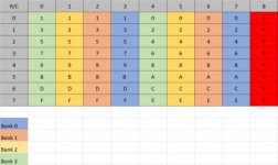
Wow.. That worked perfectly! In about 10 minutes I was able to map the entire board!

See attached map for the IC locations. When I get my next DIP socket in (tomorrow, if the Amazon Gods deliver on time), I'll swap out the C bit in bank 4 and I should be up and running!

Thank you!

Micron 2 M-B ISA Extended Memory Board 235-0140 IC Mapping.jpg
 
And I'm happy to report that did it. Replaced one IC in bank 4 at bit 12, and the card tested perfect with the thorough memory test on Checkit. Thanks for your help!

Untitled picture.jpg
 
Back
Top