• Please review our updated Terms and Rules here

Newb Question: ISA address decoding logic levels

Eudimorphodon

Veteran Member
Joined
May 9, 2011
Messages
6,959
Location
Upper Triassic
I apologize for posting such an elementary question but I'm pretty new to designing digital circuitry (I can *kind* of troubleshoot existing stuff, but it's been a while?) and I figure someone here can answer this easily off the top of their heads.

When looking at addresses on the PC bus the logic level is HIGH for a "one" bit and LOW for a "zero", correct? IE, if the computer is operating within the bottom 64K of RAM the state of A19-A16 (highest to the left) will be:

L L L L

while if it's within the page that ends right under the 256k mark they're going to be:

L L H H

And when it rolls over into the 256K block it will be:

L H L L

yes? That's what it seems to say in the hardware manual for my Tandy 1000 EX and I think I've convinced myself that's right based on scratching my head over schematics for existing boards but my rusty brain insists on getting confused by the fact that most chip enables are "LOW", not "HIGH" (IE, the intuitive state of what constitutes a zero or one is sort of flipped?) I've about gotten the point where I want to break in my newly downloaded copy of KiCad and just want to make sure I don't make stupid mistakes in interpreting truth tables.

(Disclosure, the project in question is an idea for a 640/704k memory backfill card for Tandy EX/HXes using only three chips. Nothing really new but you have to start somewhere.)
 
Last edited:
I apologize for posting such an elementary question but I'm pretty new to designing digital circuitry (I can *kind* of troubleshoot existing stuff, but it's been a while?) and I figure someone here can answer this easily off the top of their heads.

When looking at addresses on the PC bus the logic level is HIGH for a "one" bit and LOW for a "zero", correct? IE, if the computer is operating within the bottom 64K of RAM the state of A19-A16 (highest to the left) will be:

L L L L

while if it's within the page that ends right under the 256k mark they're going to be:

L L H H

And when it rolls over into the 256K block it will be:

L H L L

yes? That's what it seems to say in the hardware manual for my Tandy 1000 EX and I think I've convinced myself that's right based on scratching my head over schematics for existing boards but my rusty brain insists on getting confused by the fact that most chip enables are "LOW", not "HIGH" (IE, the intuitive state of what constitutes a zero or one is sort of flipped?) I've about gotten the point where I want to break in my newly downloaded copy of KiCad and just want to make sure I don't make stupid mistakes in interpreting truth tables.

(Disclosure, the project in question is an idea for a 640/704k memory backfill card for Tandy EX/HXes using only three chips. Nothing really new but you have to start somewhere.)

On ISA, Address and Data bus are not inverted, so logic 0 = 0V and logic 1 is +5V (or slightly less actually with TTL logic).
Enables are whatever they are indicated on the particular chip you use/need. They can be active low (and usually the name has an overbar and symbol has a little circle which indicate a negation) or active high.
Some memories and other chips can have more than one "enable" input and have mixed active low and active high enables, so you can use them to suit your circuit. For example, 6264-kind of 8Kx8 static RAMs have one active high and one active low enables that need to be both asserted (each on its enabled state) for the RAM to be selected. 74LS138 "address" decoder chip has three enable inputs and not of the same polarity...
Having both active low and active high enables on some kind of logic functions (and RAM/ROMs) could save quite a few gates on big designs of the '70s and '80s as one could usually use straight address lines as enable signals.

HTH
Frank IZ8DWF
 
On ISA, Address and Data bus are not inverted, so logic 0 = 0V and logic 1 is +5V (or slightly less actually with TTL logic).

Excellent, thank you for making that 100% clear to me.

Enables are whatever they are indicated on the particular chip you use/need. They can be active low (and usually the name has an overbar and symbol has a little circle which indicate a negation) or active high.

So, the short version of my plan revolved around using both halves of a 74xx139 dual 1-of-4 decoder like so:

1: The "a" side will be wired with A0/A1 connected to A18/A19 and E to ground so it's always cutting the total 1MB address space into 4 256k slices. The line corresponding to 40000-7FFFF will be directly used as an enable for half the 628512 RAM chip sitting on A0-A18, while the line for 80000-BFFFF feeds into the enable line for:

2: The "b" side, which has A0/A1 sitting on A16/A17. This breaks the 256k slice into 4 64K chunks. The lines corresponding the 80000, 90000, and optionally A0000 will be fed to enable on the RAM chip, while the B0000 chunk will be wasted. (I'm planning an enable/disable jumper for A0000 because even though the Tandy hardware manual says it's open I'm worried there might be some hidden hardware conflict I don't know about because of how it double-maps its video memory.)

3: The four outputs from the 74139 I'm using(*) I was planning on feeding into one half of a 7421 dual 4-input AND gate and using its output for CE on the RAM. (If I'm reading the truth table correctly a Low on any input will equal a Low on the output, and CE is Low on the SRAM chip, so I shouldn't need to invert anything?)

(I know the one weird thing about this design is the "lower" 256K block will actually be written to the upper half of the SRAM because A18 will be active, and vice-versa for the sub-blocks in the 8-A0000 range, but I can't see why that would be a problem.)

If anyone has any thoughts about whether this is a legit idea I'd love to hear them. It seems like the standard way to make RAM cards like this using a 74138 to either directly decode eight 128k blocks or tying an enable to A19 and using two of them decode 16 64K spaces. Using the two halves of a 74139 in series seemed like a sneaky shortcut to give me greater resolution for the half of the space I needed it in to get maximum backfill out of one SRAM instead. Perhaps I'm missing something catastrophic.

Side question: Do I need buffers on the data lines, or anywhere else? I've seen a number of schematics for simple SRAM cards like this that don't have any, but the latest version of the Lo-Tech 1MB card seems to have them. (But it kind of looks like it might have something to do with the XT slot 8 support??)
 
I did make an ISA SRAM card many years ago, it had 4 SRAM chips on it, but only one chip at a time would load or drive the data bus, so I didn't use any buffer on either the DATA or ADDRESS bus. On the other hand, when I was playing with DRAM chips (many of them) on a different ISA memory card, the buffers were mandatory, probably because the DRAM chips were 64 or so :)
Both cards worked for years until I decided that 386SX was a bit too slow for the modern times.
In both cases, RAM on the ISA bus was the slowest thing on earth.
Frank
 
In both cases, RAM on the ISA bus was the slowest thing on earth.

Indeed! But since the machine it's intended for is a PCjr clone I imagine it'll be good enough. :p

The only thing that has me iffy about my idea of stacking the two halves of the 74xx139 is if there might be some issue with propagation delay or the like. (Well, actually, there's plenty of other things I'm iffy about, like where I might need bypass capacitors and other analog concerns, but... baby steps.)
 
Your idea seems to be legit.
As you've mentioned accessing addresses 0x40000-0x7FFFF will access 0x40000-0x7FFFF of the SRAM and accessing addresses 0x80000-0xAFFFF will access 0x00000-0x2FFFF of the SRAM. Nothing wrong with that.

You should be fine as far as the propagation delay goes. The typical propagation delay for the 74LS139 is about 20 ns (multiply by 2 since you're chaining two 74LS139 parts together) and for the 74LS21 it is about 10 ns. Which gives a propagation delay of about 50 ns for the whole chip select logic. Modern SRAM ICs have the access time of 55-70 ns. So that gives the access time of about 120 ns.
Given that the clock period is about 210 ns (for 4.77 MHz CPU clock), and that there are about 2 clock cycles between the address output and /MEMR or /MEMW signals going inactive (when the processor or the SRAM sample the data), you have about 420 ns - much more than 120 ns...

In any case it won't hurt to use faster and lower power logic. E.g. 74ALS139 or 74AHCT139. Unfortunately it seems that 74LS21 is not readily available in these logic series. If you like, you can substitute that with much more common 74ALS08/74AHCT08, connecting the outputs of two AND gates to the inputs of the third gate.

Regarding a buffer/transceiver on the data bus - you shouldn't need it, especially that the only thing connected there is a single SRAM IC. Yet, it might be wise to plan for a 74AHCT245 or similar (I've seen some SRAMs that have CMOS input levels... and won't work reliably when connected to TTL outputs). 74*245 is fairly easy to connect: its enable pin goes to SRAM's chip select and DIR pin to /MEMR. And if you don't need it, you can just replace it with 8 wire links.

Don't forget to put a 4.7k-10k pull-up after the jumper connecting the optional 0xA0000-0xAFFFF signal to the AND gate...
 
You should be fine as far as the propagation delay goes. The typical propagation delay for the 74LS139 is about 20 ns (multiply by 2 since you're chaining two 74LS139 parts together) and for the 74LS21 it is about 10 ns. Which gives a propagation delay of about 50 ns for the whole chip select logic. Modern SRAM ICs have the access time of 55-70 ns. So that gives the access time of about 120 ns.
Given that the clock period is about 210 ns (for 4.77 MHz CPU clock), and that there are about 2 clock cycles between the address output and /MEMR or /MEMW signals going inactive (when the processor or the SRAM sample the data), you have about 420 ns - much more than 120 ns...

Awesome.

In any case it won't hurt to use faster and lower power logic. E.g. 74ALS139 or 74AHCT139. Unfortunately it seems that 74LS21 is not readily available in these logic series. If you like, you can substitute that with much more common 74ALS08/74AHCT08, connecting the outputs of two AND gates to the inputs of the third gate.

I will definitely look at ALS or HCT for the '139.

The attraction I had for the 74LS21 in particular instead of the '08 (besides it having just the right number of inputs per gate) was mostly that I was thinking I could reuse the other half of it. The two ideas I had for it were:

1: Tie the rest of the *unused* enable outputs from the '139s to it and use it to light up an LED labeled "SYSTEM" when the computer was hitting all the memory areas not mapped to the card. Blinkenlights are fun.

2: Add another SRAM, a 128K one, and another half '139 chained to the C0000-FFFFF page and use it to select the D0000 and E0000 pages to add two UMBs. (in which case I'd use the rest of the '21 to gate those those into an enable for the 128K SRAM.) But, actually, an '08 could still AND those two together even if I used three gates for the 512K, so for this the '21 doesn't have any advantage, does it. :p

Granted scenario two doesn't really produce a card much simpler than the lo-tech 1MB, it just wastes a little less memory for the same level of backfill. (With the A, D, and E pages enabled I'd be using 9/10ths of the installed RAM vs. 9/16ths. I want to leave the C-page open for future addition of an XT-IDE-type card.) For KISS reasons I should probably start with the one-chip design...

Regarding a buffer/transceiver on the data bus - you shouldn't need it, especially that the only thing connected there is a single SRAM IC. Yet, it might be wise to plan for a 74AHCT245 or similar (I've seen some SRAMs that have CMOS input levels... and won't work reliably when connected to TTL outputs). 74*245 is fairly easy to connect: its enable pin goes to SRAM's chip select and DIR pin to /MEMR. And if you don't need it, you can just replace it with 8 wire links.

Hrm. The datasheet I pulled off Jameco for the HM628512 states the chip's Hi-CMOS process is "Directly TTL compatible: All inputs and outputs" but... considering I don't have the chip in my hands yet and I might end up with something else I don't suppose it hurts to at least leave the option open. (Or at least get a chip in my hands before deciding and base it on its particular datasheet.)

Don't forget to put a 4.7k-10k pull-up after the jumper connecting the optional 0xA0000-0xAFFFF signal to the AND gate...

Yes sir! For the lines that are permanently connected the "H" level of the outputs from the '139 and '21/'08 they will be fine without help?
 
I was building some home made ISA cards for my IBM5155. I found that back in the 80's JDR micro-devices made some prototype ISA cards which had all the decoder & buffer circuits on them for practically any project. I have attached the schematic and the info. It might possibly help you. One of their projects used this to interface to an 8255-5 and 5832 rtc for a clock project.

It really does pay to use the bidirectional bus transceiver IC's 74LS245 and line driver IC's 74LS244. Then you can have a "do it all" ISA bus interface.
 

Attachments

  • jdr1.jpg
    jdr1.jpg
    86.9 KB · Views: 1
  • jdr2.jpg
    jdr2.jpg
    98.1 KB · Views: 1
Back in the day, I used the JDR ISA boards for a lot of "off the cuff" implementations mostly because of the interface logic included. I still have a couple of them.
 
Awesome.

I will definitely look at ALS or HCT for the '139.

That is AHCT... HCT is slower, about the same speed as LS

1: Tie the rest of the *unused* enable outputs from the '139s to it and use it to light up an LED labeled "SYSTEM" when the computer was hitting all the memory areas not mapped to the card. Blinkenlights are fun.

Remember that TTL logic can't source current. So connect your LED with the cathode (-) to the logic output and the anode (+) to +5V power supply (through a current limiting resistor). This actually should work just fine, since the outputs of the decoders are active LOW anyway, and that's when you want the LED to light up. You might want to do a logic AND of /MEMR and /MEMW as well... otherwise the LED will light up even then system is accessing I/O, or transitioning from one address to another. Use 470 ohm or more resistor when connecting LED directly to a logic output. Modern LEDs are bright enough (especially the true green / blue / white varieties), and they will light up with very little current flowing through them - 2 mA is more than enough.

2: Add another SRAM, a 128K one, and another half '139 chained to the C0000-FFFFF page and use it to select the D0000 and E0000 pages to add two UMBs. (in which case I'd use the rest of the '21 to gate those those into an enable for the 128K SRAM.) But, actually, an '08 could still AND those two together even if I used three gates for the 512K, so for this the '21 doesn't have any advantage, does it. :p

Granted scenario two doesn't really produce a card much simpler than the lo-tech 1MB, it just wastes a little less memory for the same level of backfill. (With the A, D, and E pages enabled I'd be using 9/10ths of the installed RAM vs. 9/16ths. I want to leave the C-page open for future addition of an XT-IDE-type card.) For KISS reasons I should probably start with the one-chip design...

I also hate to see the RAM "wasted", but using two 512 KB chips will simplify the bill of materials. By the way, if you want to make your project reproducible, AS6C4008 is a great replacement for HM628512.

Hrm. The datasheet I pulled off Jameco for the HM628512 states the chip's Hi-CMOS process is "Directly TTL compatible: All inputs and outputs" but... considering I don't have the chip in my hands yet and I might end up with something else I don't suppose it hurts to at least leave the option open. (Or at least get a chip in my hands before deciding and base it on its particular datasheet.)

I had an issue with the AS6C1008 (128 KB SRAM) chip particularly. For some reason its minimal input logic "HIGH" voltage (VIH) is specified to be VCC*0.7 = 3.5V for 5V power supply, well above minimal TTL output logic "HIGH" voltage of 2.4V, and even more than typical TTL output logic "HIGH" - 3.4V.
Surprisingly, the AS6C4008 (512 KB SRAM) has minimal input logic "HIGH" voltage of 2.4V, in other words it is TTL compatible.


For the lines that are permanently connected the "H" level of the outputs from the '139 and '21/'08 they will be fine without help?
You don't need pull-ups on the outputs of '139 and '21/'08. These outputs are not open collector or open drain, so they will supply voltage when the output logic level is "H".
 
I had an issue with the AS6C1008 (128 KB SRAM) chip particularly. For some reason its minimal input logic "HIGH" voltage (VIH) is specified to be VCC*0.7 = 3.5V for 5V power supply, well above minimal TTL output logic "HIGH" voltage of 2.4V, and even more than typical TTL output logic "HIGH" - 3.4V.
Surprisingly, the AS6C4008 (512 KB SRAM) has minimal input logic "HIGH" voltage of 2.4V, in other words it is TTL compatible.

For IC's like that in a TTL system I think the solution is just to drive those inputs with 'HCT family, because their output stages swing rail to rail, but their inputs are TTL logic level compatible.
 
Remember that TTL logic can't source current. So connect your LED with the cathode (-) to the logic output and the anode (+) to +5V power supply (through a current limiting resistor). This actually should work just fine, since the outputs of the decoders are active LOW anyway, and that's when you want the LED to light up.

Yeah, that's how I was thinking I needed to do it based on some pretty rusty memories, but thank you for confirming that'll work.

You might want to do a logic AND of /MEMR and /MEMW as well... otherwise the LED will light up even then system is accessing I/O, or transitioning from one address to another.

I'm not sure I cared too much how accurate it was, it'd just be for laughs. I do think maybe I'm sold on using the '08 as you suggested instead of the '21, because if I do the LED thing I could just run two LEDs, a "SYS" for when the addresses are between either 0-3FFFF or C0000-FFFFF using the one spare AND gate on the '08 and a "VID" LED by tying it directly to the "B-page" output from the second half of the '139. That would tie up all the loose ends.

I also hate to see the RAM "wasted", but using two 512 KB chips will simplify the bill of materials. By the way, if you want to make your project reproducible, AS6C4008 is a great replacement for HM628512.

Thank you for tipping me off to the AS6C4008. Digi-Key seems to have them in stock for less than Jameco wants for a 128K part. (Or, to put it another way, only a third of the cost of the HM628512.

I'm not sure I really care about getting the UMBs because, well, it's a 1000 EX and I don't anticipate using something that has really RAM-hungry drivers like a network card or CD-ROM, so at least for Revision A I think I'll concentrate on the brain-dead version. I am curious to see if the A0000 page will actually work, even just that extra 64k would be icing on the cake. (I believe there's a memory expansion out there for the PCjr that fills that page and works, and the Tandy manual *does* say it's free so... fingers crossed? I assume I'll need to find some sort of driver to enable it, the BIOS won't just automatically count it out.)

You don't need pull-ups on the outputs of '139 and '21/'08. These outputs are not open collector or open drain, so they will supply voltage when the output logic level is "H".

Cool.

Now to wrap my head around KiCad. I see a steep learning curve in my future.
 
Not an elementary question at all. This is real top end stuff. Beyond me. Designing digital circuity... you need to go to college for that I presume.
 
Not an elementary question at all. This is real top end stuff. Beyond me. Designing digital circuity... you need to go to college for that I presume.

Not really.. Microprocessor interfacing is pretty simple.
There were lots of easy to follow books for building things in the late 70s and 80s.
I built my first microprocessor (6802) based terminal when I was in high school.
I built my first terminal by making copies of the TTL boards in an Ann Arbor terminal before that.
 
Three weeks later...

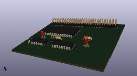
After spending a hunk of the weekend learning the most rudimentary basics of KiCad I've turned out a schematic and a "Maybe it'd work" PCB layout for my proposed simple Tandy 1000EX/HX memory card. (I'm thinking it deserves to be called a "Tandy Minus" memory card vs. the "Plus" of the original.) Witness KiCad's ridiculous 3D rendering feature in action:

TandyRam3d.jpg

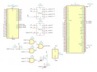
If any gurus would be willing to share a bit more wisdom I have a few more dumb questions to throw out. Here is the schematic I put together:

tandyram.jpg

I *think* I have the wiring correct for the 74x139, although KiCad's representation of the chip in their symbol table uses a different naming convention for the inputs than the data sheet, which had me scratching my head for while. Also the naming convention for the pins on the Tandy Plus connector is kind of a mix of the standard ISA names and the names in the Tandy 1000EX technical manual, which might be confusing. (I copied the pre-defined 8-bit ISA symbol as the starting point.) The main questions I have are:

1: The "analog" elements of digital electronics are not my strong point. I didn't incorporate any bypass capacitors into the schematic or PCB layout, is it likely I'll need them? The dimensions of the prototype board as I rendered it are about 2.5" by 3.5", which is significantly smaller than a regular Plus card, if that makes a difference.

2: How important is it for things like data and address line traces to be of the same length for a board operating at a maximum of 7.16mhz? (On the scale from "vital" to "don't worry about it"? I'll be blunt, manually routing traces is at this point not one of my talents so the PCB layout is kind of a mess.

3: A harebrained idea I came up with to allow further expansion was to use a stacking header like used with Arduino and Raspberry Pi shields to carry the bus *through* the card instead of doing the two alternating tall/short connectors like the original Plus board. (The 3D rendering obviously has the wrong header on it, in the real world it'll need a female socket on the bottom.) I found that 2x18 and 2x13 stacking headers are off the shelf parts and if I'm doing the math right that adds up to a 2x31. Is there any reason that wouldn't work, other than the height might not be compatible with original Plus boards?

(The only Plus board I have is the 1200 baud modem, which is probably pretty useless to me unless there's some way to lobotomize it into enough of a serial port to drive a mouse. Therefore compatibility with original boards isn't a huge priority)
 
1: The "analog" elements of digital electronics are not my strong point. I didn't incorporate any bypass capacitors into the schematic or PCB layout, is it likely I'll need them? The dimensions of the prototype board as I rendered it are about 2.5" by 3.5", which is significantly smaller than a regular Plus card, if that makes a difference.

2: How important is it for things like data and address line traces to be of the same length for a board operating at a maximum of 7.16mhz? (On the scale from "vital" to "don't worry about it"? I'll be blunt, manually routing traces is at this point not one of my talents so the PCB layout is kind of a mess.
On these two questions the Gold standard is to have one 0.1uF monolithic ceramic capacitor per IC close to its power rails, but many authors say one capacitor per two IC's is ok and I have seen at lot less used at the designer's peril.

On a pcb, with frequencies in the order of 15MHz or less there is usually negligible trouble with pcb track length with both TTL and or Cmos. At much higher frequencies its a whole other story. Also if you are transmitting pulses between pcb's on ribbon cable etc, as the capacitance can be significant, one easy cure is to put 22R resistors in series with line driver outputs which helps to dampen any resonances and tuning effects.There have also been arguments to terminate the input end with a pair of resistors on the 5V supply that set a H logic level and have an overall Thevenin resistance (their parallel value) to match the source impedance, so as to reduce unwanted reflections and improve the system's maximum operating frequency.
 
Thank you for the feedback. I'll see about incorporating some bypass caps between 5v and ground near each IC.

I guess I'm not going to worry too much about the effects you mentioned with ribbon cables, etc, as the longest traces are only about three inches long and the only connector for this version is the bus connector, which even with a stacking connector will only be about an inch.
 
Driving long (10m and longer) parallel data cables is an art when frequencies go up. You not only have to worry about impedance matching and crosstalk, but skewing effects.

For moderate frequencies < 2MHz, I prefer open-collector/drain drivers on the source end and 220/330 termination on the destination, preferably feeding a Schmitt-trigger receiver. Higher frequencies are better handled with differential drive--keeps the issue of crosstalk and common-mode noise under control. There's a slight edge to be gained with twisted-pair ribbon cable, rather than the flat variety.

Of course, everything is serial nowadays...
 
Back
Top